Manufacturing Method Of Semiconductor Device And Film Deposition System

a manufacturing method and film deposition technology, applied in chemical vapor deposition coating, coating, metallic material coating process, etc., can solve the problems of inability to remove fluorine-added carbon film, increase the dielectric constant of the dielectric constant, and reduce the density of the surface of the fluorine-added carbon film. excellent

Inactive Publication Date: 2008-10-16
TOKYO ELECTRON LTD
View PDF10 Cites 77 Cited by
  • Summary
  • Abstract
  • Description
  • Claims
  • Application Information

AI Technical Summary

Benefits of technology

[0009]The present invention has been made in view of the above context. It is the object of the present invention to provide a manufacturing method of a semiconductor device in which an excellent adhesion between the fluori

Problems solved by technology

Further, when the resist film is removed by ashing by means of an oxygen plasma, the fluorine-added carbon film is undesirably removed.
However, use of these materials is disadvantageous in that a higher relative dielectric constant thereof increases a relative dielectric constant of the overall interlayer dielectric films.
However, there is a problem with the SiCO film.
Thus, denseness of a surfac

Method used


Image

  • Manufacturing Method Of Semiconductor Device And Film Deposition System
  • Manufacturing Method Of Semiconductor Device And Film Deposition System
  • Manufacturing Method Of Semiconductor Device And Film Deposition System

Examples


example 1

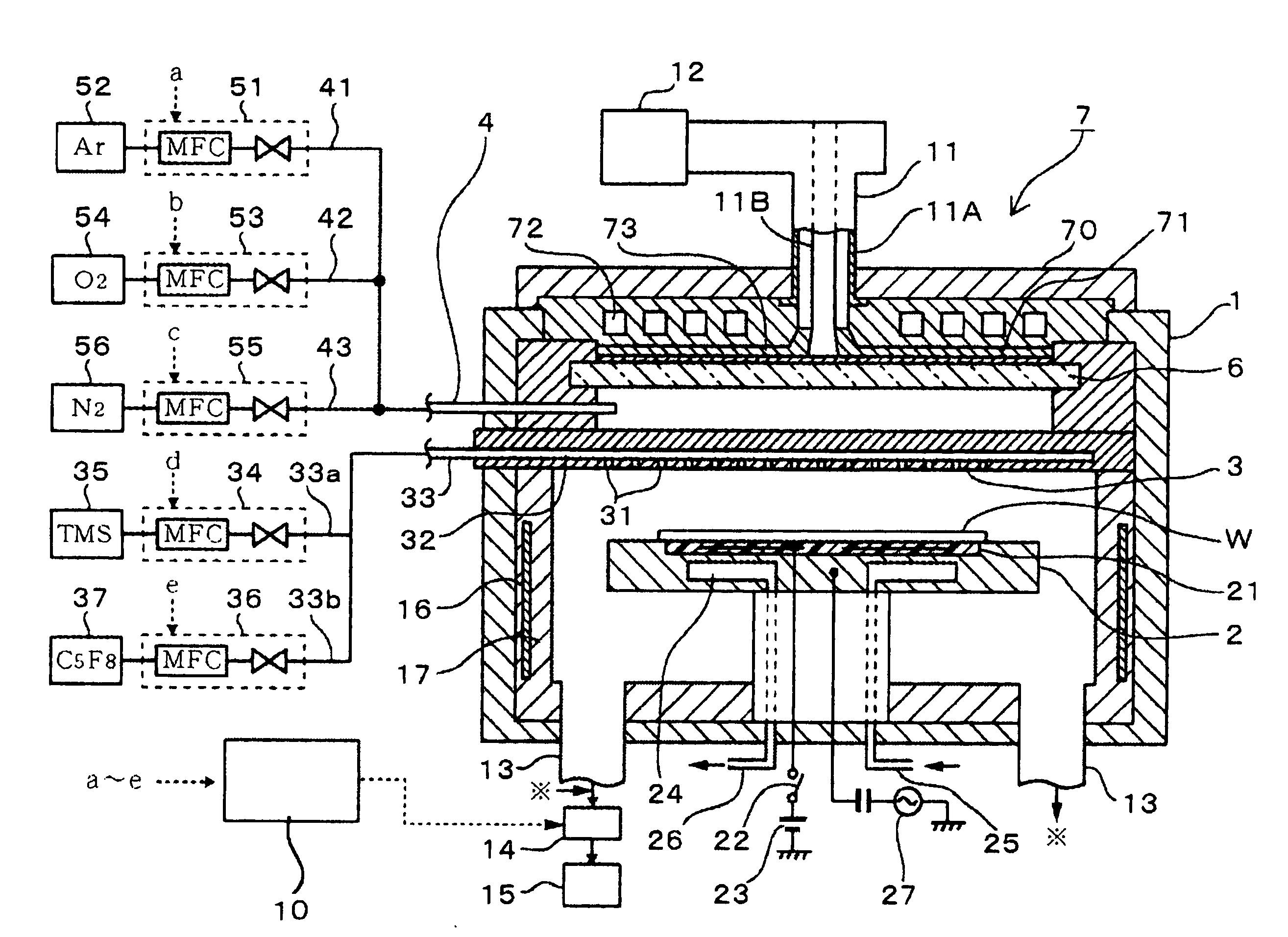
[0114]Example 1 corresponds to the second embodiment. With the use of the plasma processing apparatus shown in FIG. 1, a fluorine-added carbon film of 120 nm in thickness was deposited on a silicon bare wafer. The film deposition conditions were as follows: A power of a microwave was set at 3000 W, a process pressure was set at 10.6 Pa (80 mTorr), a temperature of the wafer was set at 380° C., and flow rates of C5F8 gas and Ar gas were set at 200 sccm and 100 sccm, respectively.

[0115]Then, an SiCN film of 50 nm in thickness was deposited on the fluorine-added carbon film by using the same plasma processing apparatus. The film deposition conditions were as follows: A power of a microwave was set at 1500 W, a process pressure was set at 39.9 Pa (300 mTorr), and a temperature of the wafer was set at 380° C. TMS gas (vapor) and Ar gas were supplied at flow rates of 40 sccm and 80 sccm, respectively. In addition, nitrogen gas was supplied at a flow rate of 50 sccm, after 5 seconds had pa...

example 2

[0116]Example 2 corresponds to the first embodiment. Similar to Example 1, a fluorine-added carbon film and an SiCN film were sequentially deposited on a silicon bare wafer. However, in this example, a thickness of the SiCN film was 5 nm, in view of a function of the SiCN film as a protective layer. Then, an SiCO film of 50 nm in thickness was deposited on the SiCN film by using the same plasma processing apparatus. The film deposition conditions were as follows: A power of a microwave was set at 1500 W, a process pressure was set at 33.3 Pa (250 mTorr), and a temperature of the wafer was set at 380° C. TMS gas and Ar gas were supplied at flow rates of 40 sccm and 200 sccm, respectively. In addition, oxygen gas was supplied at a flow rate of 10 sccm, after 5 seconds had passed from the beginning of the supply of the TMS gas and the Ar gas.

example 3

[0117]Similar to Example 2, an SiCN film and an SiCO film were deposited on a fluorine-added carbon film in this order. However, in depositing the SiCN film, the initial step of supplying only TMS gas and Ar gas was not carried out, but TMS gas, Ar gas, and nitrogen gas were supplied from the beginning.


PUM

PropertyMeasurementUnit
Dielectric polarization enthalpyaaaaaaaaaa

Abstract

A dielectric film (91) made of CF is deposited on a substrate. A protective layer comprising an SiCN film (93) is formed on the dielectric film (91). A film (94) serving as a hardmask made of SiCO is deposited on the protective layer by a plasma containing active species of silicon, carbon, and oxygen. When the protective layer is formed, an SiC film (92) is deposited on the dielectric film (91) by a plasma containing active species of silicon and carbon, and thereafter the SiCN film (93) is deposited on the SiC film (92) by a plasma containing active species of silicon, carbon, and nitrogen.

Description

FIELD OF THE INVENTION[0001]The present invention relates to a manufacturing method of a semiconductor device having a dielectric film made of fluorine-added carbon, and a film deposition system for manufacturing such a semiconductor device.BACKGROUND ART[0002]One of the techniques for achieving a higher degree of integration of a semiconductor device is to multilayer a wiring. When forming a multilayered wiring structure, an n-th wiring layer and an (n+1)-th wiring layer are connected to each other through a conductive layer, and films called “interlayer dielectric films” are deposited on an area other than the conductive layer. A representative interlayer dielectric film is an SiO2 film. With a view to realizing a higher speed of an operation of the device, a lower relative dielectric constant of the interlayer dielectric film has been recently demanded. In consideration of this demand, a fluorine-added carbon film (fluorocarbon film), which is a compound of carbon (C) and fluorin...

Claims


Application Information

Patent Timeline
IPC IPC(8): H01L21/31C23C16/513H01L21/311H01L21/312H01L21/314H01L21/316H01L21/768
CPCH01L21/02118H01L21/02126H01L21/02167H01L21/02274H01L21/31144H01L21/3127H01L21/3143H01L21/31633H01L21/76811H01L21/76832H01L21/76835
Inventor KOBAYASHI, YASUONISHIZAWA, KENICHIKAMESHIMA, TAKATOSHIMATSUOKA, TAKAAKI
Owner TOKYO ELECTRON LTD
Why Eureka
Try Eureka