Scanning Probe Microscope System

a scanning probe and microscope technology, applied in the direction of instruments, material analysis using wave/particle radiation, nuclear engineering, etc., can solve the problems of difficult to achieve atomic scale spatial resolution, and no way to establish a technique which is very difficult to achiev

Inactive Publication Date: 2008-10-23
RIKEN
View PDF2 Cites 12 Cited by
  • Summary
  • Abstract
  • Description
  • Claims
  • Application Information

AI Technical Summary

Benefits of technology

[0026]Since the present invention is constructed as described above, it results in such excellent advantages that an observation by...

Problems solved by technology

Accordingly, there is such a problem that electrons generated in a wide range are collected in accordance with the techniques disclosed in the non-patent literary documents 1 and 2, so that the spatial resolution stays in an order of 10 μm.
Such problem is a principle problem impartible with respect to such conventional technique, so that it is very difficult to obtain atomic scale spatial resolution.
In these...

Method used


Image

  • Scanning Probe Microscope System
  • Scanning Probe Microscope System
  • Scanning Probe Microscope System

Examples


Embodiment Construction

[0056]In the following, an example of the embodiment of the scanning probe microscope system according to the present invention will be described in detail by referring to the accompanying drawings.

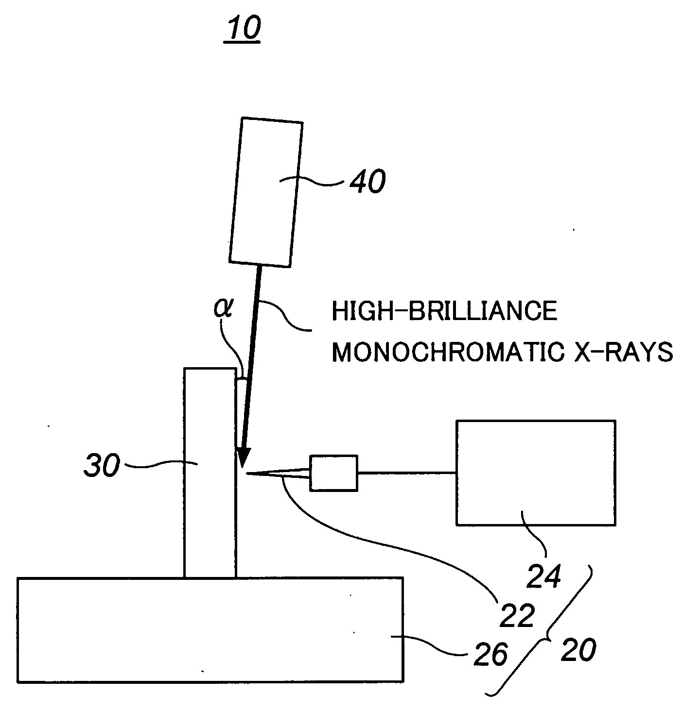
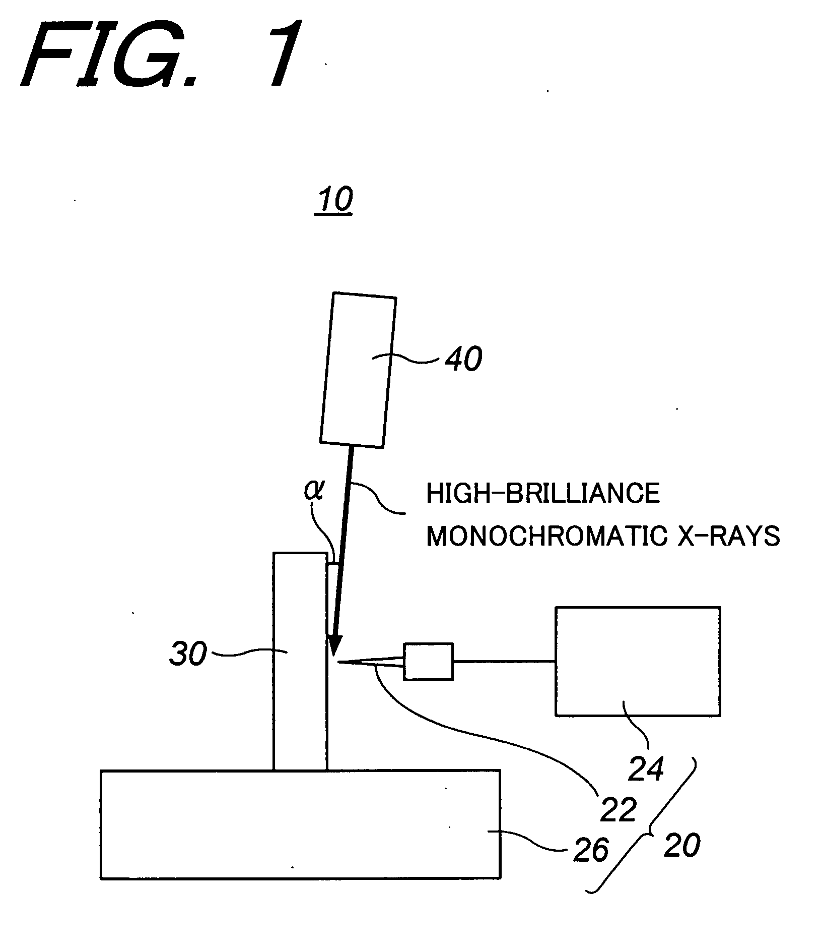
[0057]FIG. 1 is a conceptual, constitutional, explanatory diagram showing the principle of the scanning probe microscope according to an example of an embodiment of the present invention.

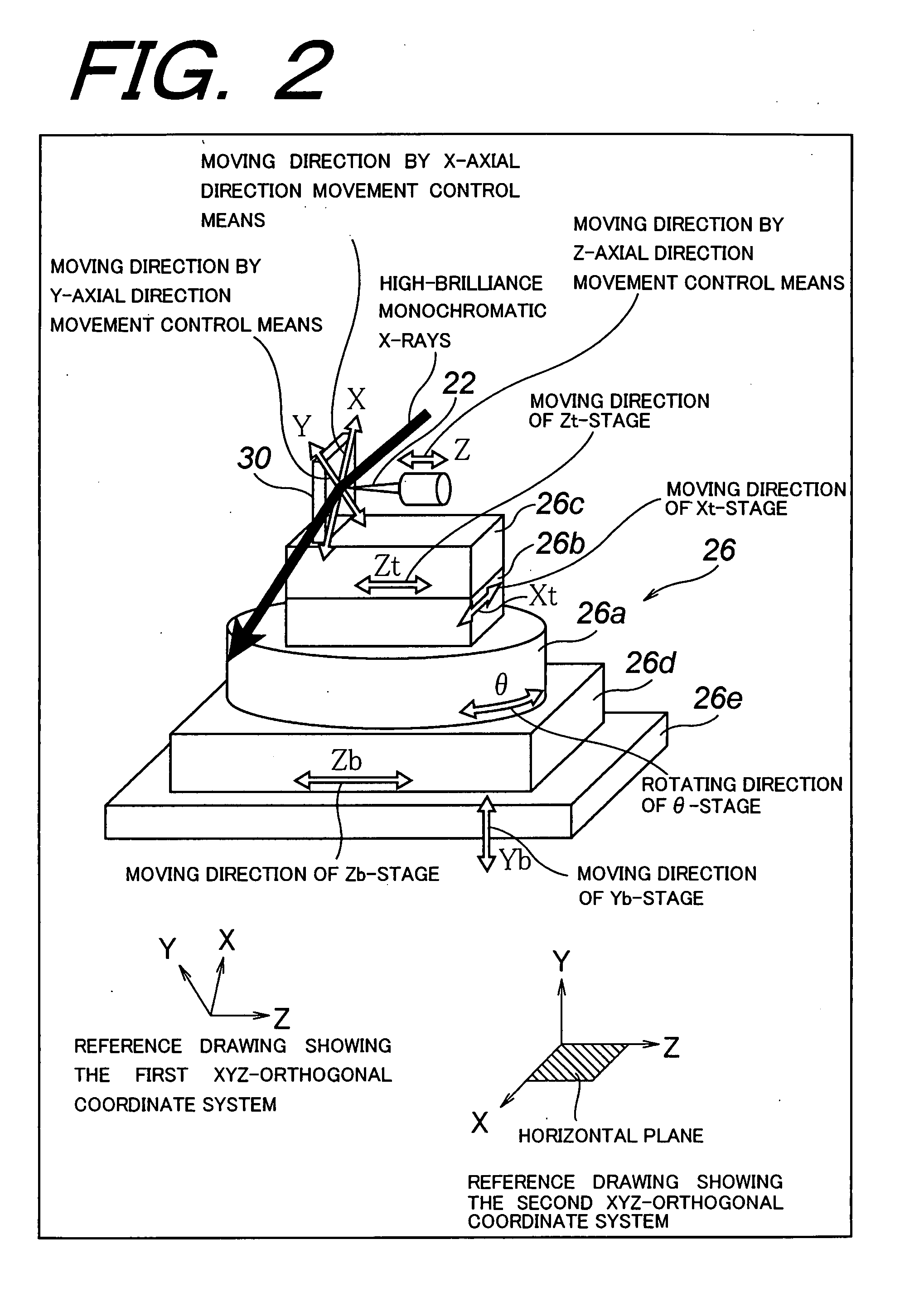
[0058]The scanning probe microscope system 10 comprises a scanning probe microscope 20 including a probe 22 opposed to a sample 30 being a measurement object, processing means 24 for detecting and processing a physical quantity through the probe 22, and an alignment mechanism 26 (wherein the alignment mechanism 26 will be mentioned later by referring to FIG. 2. In the embodiment, the alignment mechanism 26 makes the sample 30 to be moved with respect to the probe 22 and the incident position of the beam of the high-brilliance monochromatic X-rays, whereby the relative movement of the sample 30, the probe ...


PUM


Abstract

A scanning probe microscope system capable of identifying an element with atomic scale spatial resolution comprises: an X-ray irradiation means for irradiating a measurement object with high-brilliance monochromatic X-rays having a beam diameter smaller than 1 mm; a probe arranged to oppose to the measurement object; a processing means for detecting and processing a tunneling current through the probe; and a scanning probe microscope having an alignment means for relatively moving the measurement object, the probe, and the incident position of the high-brilliance monochromatic X-rays to the measurement object.

Description

TECHNICAL FIELD[0001]The present invention relates to a Scanning Probe Microscope (SPM) system, and more particularly to a scanning probe microscope system wherein a microscopy for scanning a microprobe represented by Scanning Tunneling Microscope (STM) or Atomic Force Microscope (AFM) is applied.BACKGROUND TECHNOLOGY[0002]Most of conventional nanostructure evaluation techniques are concerned only to the one which provides limited individual information. A nanostructure itself has been construed by judging synthetically the individual information obtained respectively from a plurality of nanostructure evaluation techniques.[0003]Among these conventional nanostructure evaluation techniques, since a scanning probe microscope system has atomic scale spatial resolution so that spatial information can be obtained, such scanning probe microscope system may be applied also to the observation for a system exhibiting no periodicity. As a result, the scanning probe microscope system has contr...

Claims


Application Information

Patent Timeline
IPC IPC(8): G21K7/00G01B21/30G01N23/223G01Q10/02G01Q30/02G01Q60/10G01Q70/12
CPCB82Y35/00G01Q60/12G01Q30/02G01N23/225
Inventor SAITO, AKIRAAONO, MASAKAZUKUWAHARA, YUJIMARUYAMA, JYUNPEIMANABE, KEN
Owner RIKEN
Why Eureka
Try Eureka