Contact Scheme for MOSFETs

a technology of contact scheme and mosfet, which is applied in the direction of semiconductor devices, semiconductor/solid-state device details, electrical apparatus, etc., can solve the problems of increasing the difficulty of forming contacts to fin field-effect transistors (finfets), increasing the difficulty of forming contacts to fins, so as to reduce the aspect ratio of contacts and reduce manufacturing costs

Inactive Publication Date: 2008-10-23
TAIWAN SEMICON MFG CO LTD
View PDF18 Cites 122 Cited by
  • Summary
  • Abstract
  • Description
  • Claims
  • Application Information

AI Technical Summary

Benefits of technology

[0011]The advantageous features of the present invention include reduced aspect ratios of contacts and reduced manufacturing cost due to the combination of forming contacts and forming gate electrodes.

Problems solved by technology

Accordingly, the aspect ratios of contacts continuously increase, causing the contact formation process to be more and more difficult.
The difficulty is further increased for forming contacts to Fin field-effect transistors (FinFET).
However, it is difficult to form contacts to fins 2.
However, landing pads 6 themselves occupy chip area, and hence such a solution defeats the purpose of forming FinFETs, which is to save chip area.

Method used


Image

  • Contact Scheme for MOSFETs
  • Contact Scheme for MOSFETs
  • Contact Scheme for MOSFETs

Examples


Embodiment Construction

[0019]The making and using of the presently preferred embodiments are discussed in detail below. It should be appreciated, however, that the present invention provides many applicable inventive concepts that can be embodied in a wide variety of specific contexts. The specific embodiments discussed are merely illustrative of specific ways to make and use the invention, and do not limit the scope of the invention.

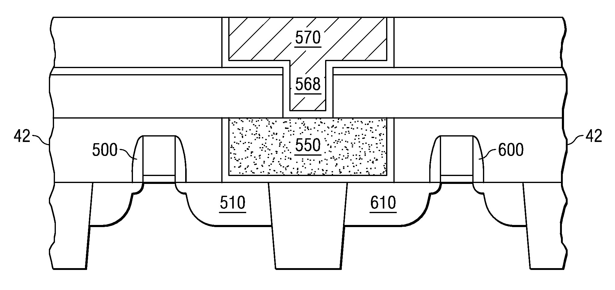
[0020]A novel contact structure and the method of forming the same are presented. The intermediate stages of manufacturing a preferred embodiment of the present invention are illustrated. The variations of the preferred embodiment are then discussed. Each figure may have a suffix A, B or C, indicating different views of a same structure. Throughout the various views and illustrative embodiments of the present invention, like reference numbers are used to designate like elements.

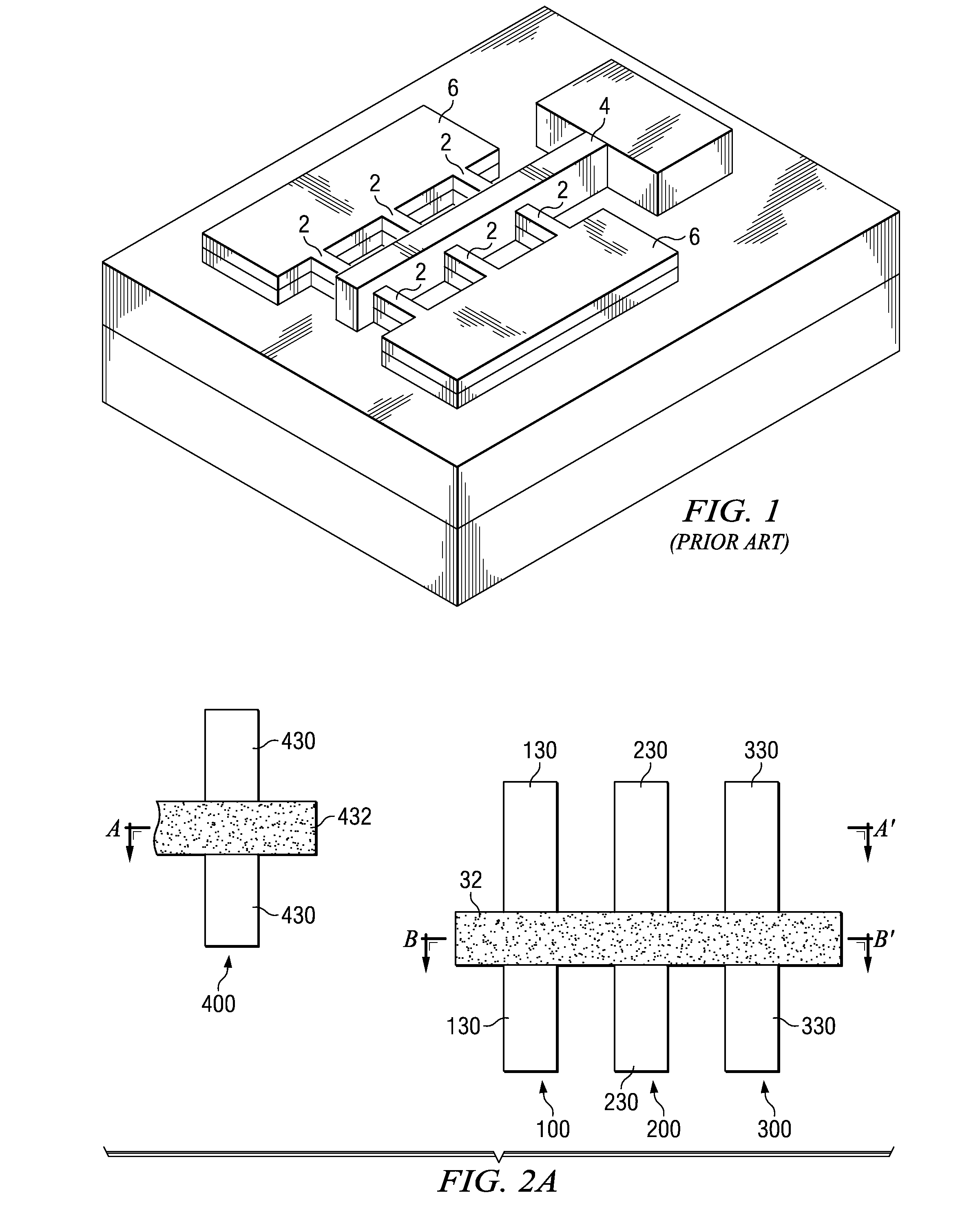
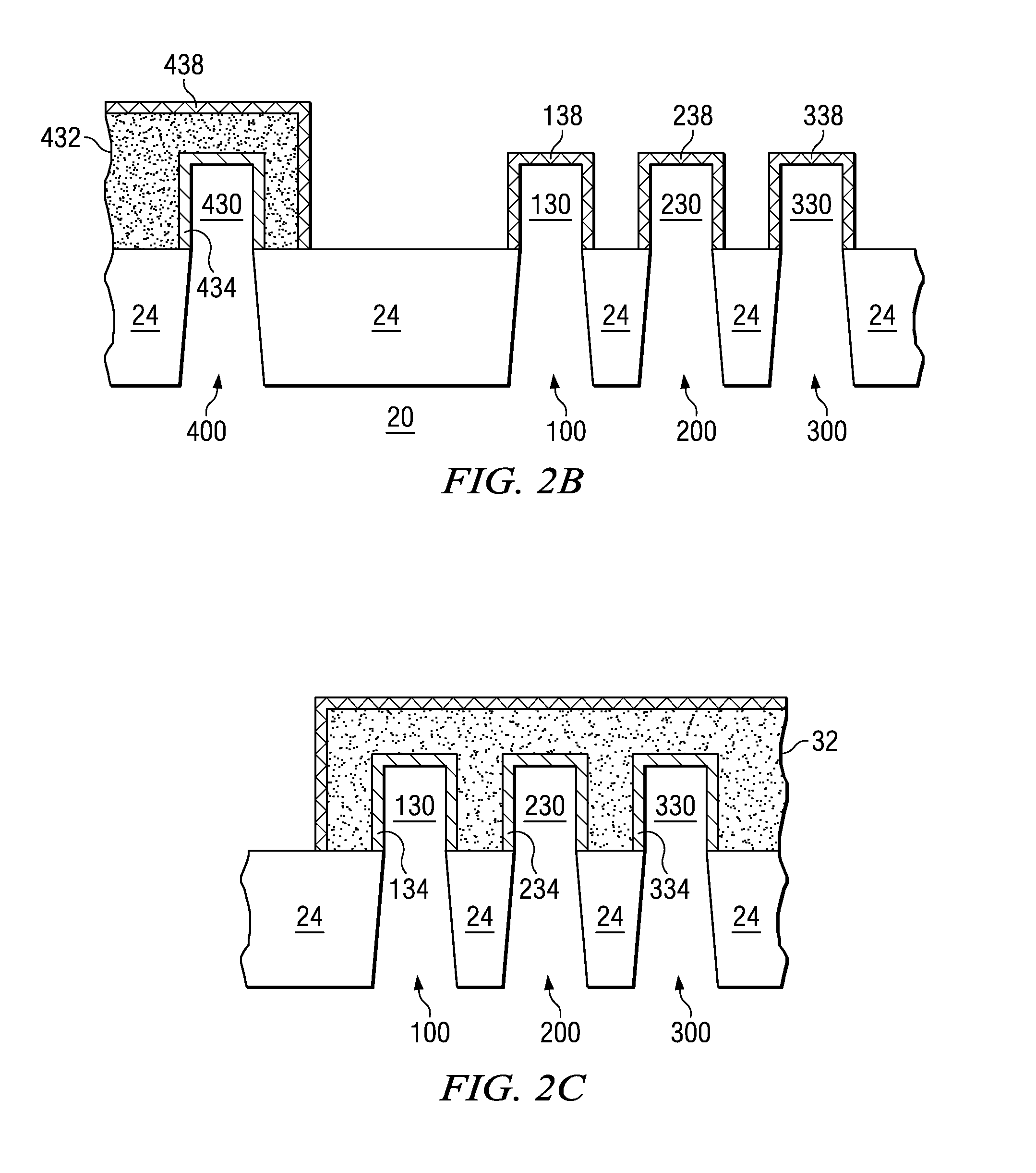
[0021]FIGS. 2A through 8 illustrate a first embodiment of the present invention. FIG. 2A illustrate...


PUM


Abstract

A semiconductor structure and methods of forming the same are provided. The semiconductor structure includes a semiconductor substrate; a first inter-layer dielectric (ILD) over the semiconductor substrate; a contact extending from a top surface of the first ILD into the first ILD; a second ILD over the first ILD; a bottom inter-metal dielectric (IMD) over the second ILD; and a dual damascene structure comprising a metal line in the IMD and a via in the second ILD, wherein the via is connected to the contact.

Description

[0001]This application claims the priority of the following provisionally filed U.S. patent application: Application Ser. No. 60 / 925,046, filed Apr. 18, 2007, entitled “3-Dimensional Device Design Layout,” which patent application is incorporated herein by reference.TECHNICAL FIELD[0002]This invention relates generally to integrated circuits, and more particularly to contact formation schemes, and even more particularly to the contacts for connecting Fin field-effect transistors (FinFET).BACKGROUND[0003]In modern integrated circuits, semiconductor devices are formed on semiconductor substrates, and are connected through metallization layers. The metallization layers are connected to the semiconductor devices through contacts, also referred to as contact plugs. Also, external pads are connected to the semiconductor devices through the contacts.[0004]Typically, the formation process of contacts includes forming an inter-layer dielectric (ILD) over semiconductor devices, forming contac...

Claims


Application Information

Patent Timeline
Patent Type & Authority Applications(United States)
IPC IPC(8): H01L29/78H01L21/8238
CPCH01L21/76807H01L21/76895H01L21/76897H01L21/823431H01L21/823437H01L21/823475H01L29/41791H01L29/66795H01L29/785H01L2029/7858
Inventor CHUANG, HARRYTHEI, KONG-BENGLIANG, MONG SONGKAO, JUNG-HUICHUNG, SHENG-CHENCHENG, CHUNG LONGLIAO, SHUN-JANG
Owner TAIWAN SEMICON MFG CO LTD
Why Eureka
Try Eureka