Circuit arrangement having a free-wheel diode

a diode and circuit technology, applied in the field of circuit arrangement, can solve the problems of pnd failure, noise cannot be suppressed, capacitor and inductance components in a circuit resonating to generate noise, etc., and achieve the effect of suppressing noise and suppressing nois

Inactive Publication Date: 2008-10-23
HITACHI LTD
View PDF4 Cites 37 Cited by
  • Summary
  • Abstract
  • Description
  • Claims
  • Application Information

AI Technical Summary

Benefits of technology

[0011]The present invention has been made in view of the above technical circumstances. An object of the present invention is to reduce conducting loss of an existing conversion circuit while suppressing noise in the circuit.
[0021]The present invention has been outlined above. According to the present invention, the SBD and PND are basically connected in parallel with each other as separate chips. Therefore, the SBD and PND independently operate with a voltage equally applied to them. Further, since the present invention is used near a current region where the forward voltages of the SBD and PND are equal, noise can be suppressed without sacrificing the excellent recovery characteristics of the SBD.
[0022]The present invention makes it possible to suppress noise in an existing conversion circuit.

Problems solved by technology

In an MPS device or other similar device in which only the SBD operates in a normal state, however, the aforementioned capacitance and inductance components in a circuit resonate to generate noise.
In the above-mentioned MPS structure, however, noise cannot be suppressed because the PND does not operate in a normal operation region and substantially no recovery current flows.
As a result, the PND fails to operate even when the applied voltage is higher than the built-in potential of a PN junction.

Method used


Image

  • Circuit arrangement having a free-wheel diode
  • Circuit arrangement having a free-wheel diode
  • Circuit arrangement having a free-wheel diode

Examples


first embodiment

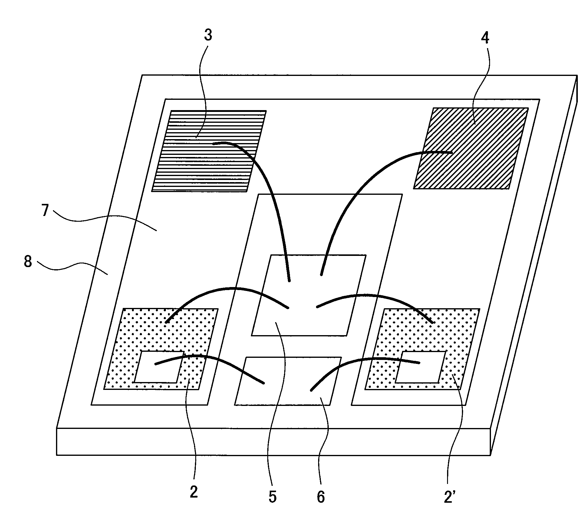
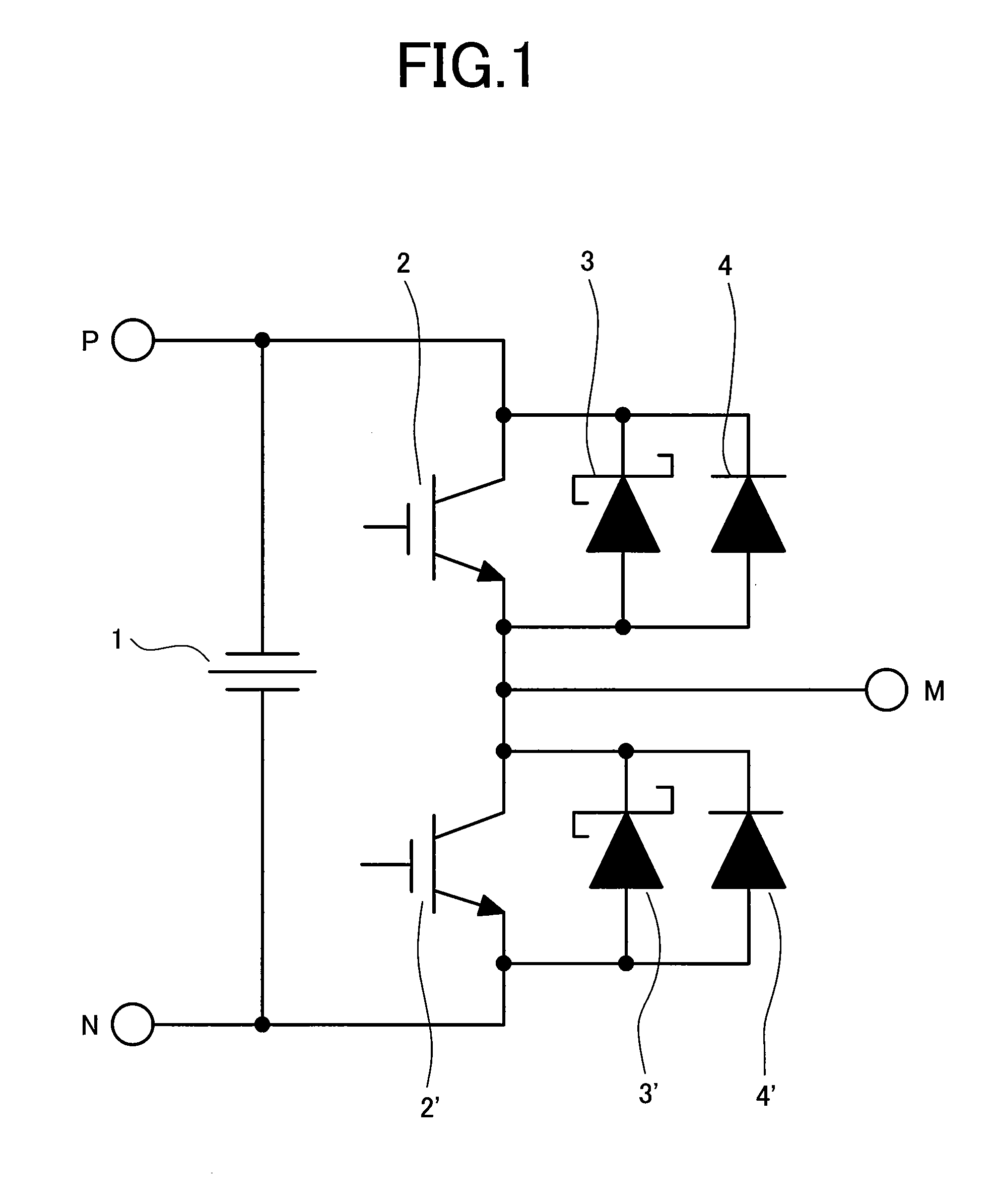
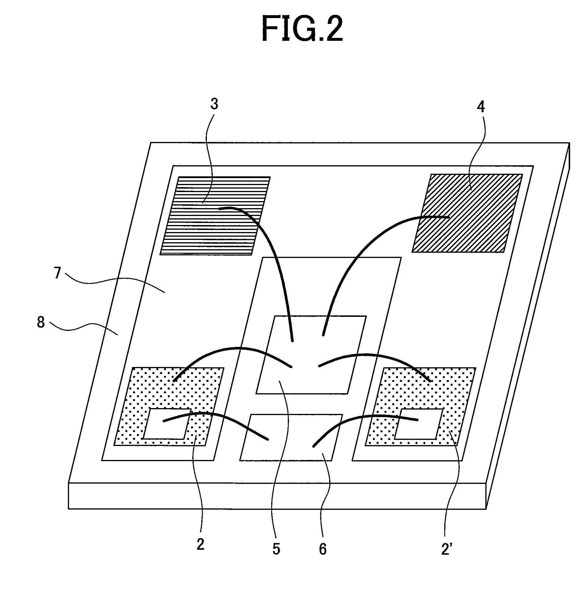
[0034]FIG. 1 illustrates the first embodiment and shows a main part of a circuit diagram depicting a power module that is used as an inverter circuit. FIG. 2 is a perspective view illustrating a part of the power module. Switching devices Si-IGBT 2 and Si-IGBT 2′ in FIG. 2 correspond to an IGBT 2 in FIG. 1. In the power module, an SiC-SBD 3 and Si-PND 4 are connected in parallel with the Si-IGBT 2. Both ends of the Si-IGBT 2 are connected to a power supply of the inverter circuit. Elements of the inverter circuit are mounted on a circuit board 8 and arranged as shown in FIG. 2. FIG. 2 shows only a part of a circuit and does not depict the entire circuit. Reference numerals in FIG. 2 correlate to those in FIG. 1. The reference numeral 5 denotes an emitter terminal. The reference numeral 6 denotes a gate terminal. The reference numeral 7 denotes a collector terminal.

[0035]The operation of the present embodiment will now be briefly described. In a three-phase inverter circuit, two seri...

second embodiment

[0040]the present invention will now be described. The second embodiment is an example of a circuit arrangement including at least one switching device and a free-wheel diode connected in parallel with the switching device, wherein the free-wheel diode is formed by connecting two or more series-connected PiN diodes in parallel with a Schottky barrier diode that uses a semiconductor material having a wider band gap than silicon as a base material; wherein the PiN diodes use a semiconductor material having a wider band gap than silicon as a base material; and wherein the Schottky barrier diode and the PiN diodes are separate chips.

[0041]FIG. 7 illustrates the second embodiment and shows a part of a circuit diagram depicting a power module that is used as an inverter circuit. The example shown in FIG. 7 differs from the one shown in FIG. 1 in that a PiN diode made of a semiconductor material having a wider band gap than silicon is used in place of a PiN diode made of a silicon semicond...


PUM


Abstract

An object of the present invention is to reduce the conducting loss of an existing conversion circuit while suppressing its noise. The present invention is typically a circuit arrangement includes at least one switching device and a free-wheel diode connected in parallel with the switching device. The free-wheel diode is formed by connecting a silicon PiN diode in parallel with a Schottky barrier diode that uses a semiconductor material having a wider band gap than silicon as a base material. The silicon PiN diode and Schottky barrier diode are separate chips.

Description

CLAIM OF PRIORITY[0001]The present application claims priority from Japanese application JP 2007-111605 filed on Apr. 20 2007, the content of which is hereby incorporated by reference into this application.BACKGROUND OF THE INVENTION[0002]1. Field of the Invention[0003]The present invention relates to a circuit arrangement having at least one switching device and a free-wheel diode connected in parallel with the switching device. The present invention is particularly useful when it is applied to a power semiconductor module having a rectifying device.[0004]2. Description of the Related Art[0005]Semiconductor power modules are used in various fields as a device that composes an inverter. Particularly, power modules that use a Si-IGBT (Insulated Gate Bipolar Transistor) as a switching device and a Si-PiN diode (hereinafter referred to as a Si-PND) as a free-wheel diode exhibit low loss and high blocking voltage and are used in a wide variety of fields such as railroads and consumer el...

Claims


Application Information

Patent Timeline
Patent Type & Authority Applications(United States)
IPC IPC(8): H01L27/00
CPCH01L25/18H01L2924/13062H03K17/16H03K17/567H03K17/687H03K17/732H03K17/74H03K2217/0036H01L2224/48091H02M7/003H01L2924/1305H01L2924/12032H01L2924/13055H01L2924/1301H01L2924/13091H01L2924/30107H01L2924/00014H01L2924/00
Inventor SHIMIZU, HARUKAISHIKAWA, KATSUMINAGASU, MASAHIROTSUGAWA, DAI
Owner HITACHI LTD
Why Eureka
Try Eureka