Integrated circuit having compact high-speed bus lines for optical signal

Inactive Publication Date: 2008-10-23
CHUNGHWA TELECOM CO LTD
View PDF5 Cites 4 Cited by
  • Summary
  • Abstract
  • Description
  • Claims
  • Application Information

AI Technical Summary

Benefits of technology

[0009]A primary objective of the present invention is to provide an integrated circuit having compact high-speed bus lines for optical signals which is low cost and ease of use.
[0010]A secondary objective of the present invention is to provide an integrated circuit having compact high-speed bus lines for optical signals that is capable of solving disadvantages such as highly complicated structure and high cost due to processes difficulties, rendering that the use of optoelectronic components would be easy as using an IC chip in a circuit board.
[0012]A further objective of the present invention is to provide a compact high-speed optical bus line for use in a rotatable cover of the cell phones (instead of present flexible circuit board) and of the notebooks.
[0013]To achieve the above objectives, an integrated circuit having compact high-speed optical signal bus lines of the present invention uses a fiber hole array for solving the technical bottlenecks concerning optical-fiber package of array wafer for increasing productions and reducing manufacturing cost. Therefore, the integrated circuit with interconnection buses for optical signals can be produced in a simplified way, mainly comprising:

Problems solved by technology

Due to strong demand of high-speed broadband, a design of preventing interferences incurred by transmitting broadband signals between high-density copper wires has become difficult.
The existing apparatuses for optical signal interconnecting are complex and cause high manufacturing cost than average electronic products, thus which cannot be efficiently utilized.
Most of the short distance optical signal connections that employed point-to-point optical interface connections which is difficult in manufacturing an ultra-compact bus line, especially, is even harder for optical fiber package in connection with LD Array and PIN Array.
However, the fabrication of optical component is much more difficult than that of IC chips.
Also, positioning optical waveguides and other optical transmitting paths have to be calibrated within a range of 1*m. It still requires manual operation and thus cannot be produced in a great number, resulting relatively high cost.
Those prototypes developed by the above-mentioned companies are difficult to manufacture, and are expensive and devoid of flexibility.

Method used


Image

  • Integrated circuit having compact high-speed bus lines for optical signal
  • Integrated circuit having compact high-speed bus lines for optical signal
  • Integrated circuit having compact high-speed bus lines for optical signal

Examples


Embodiment Construction

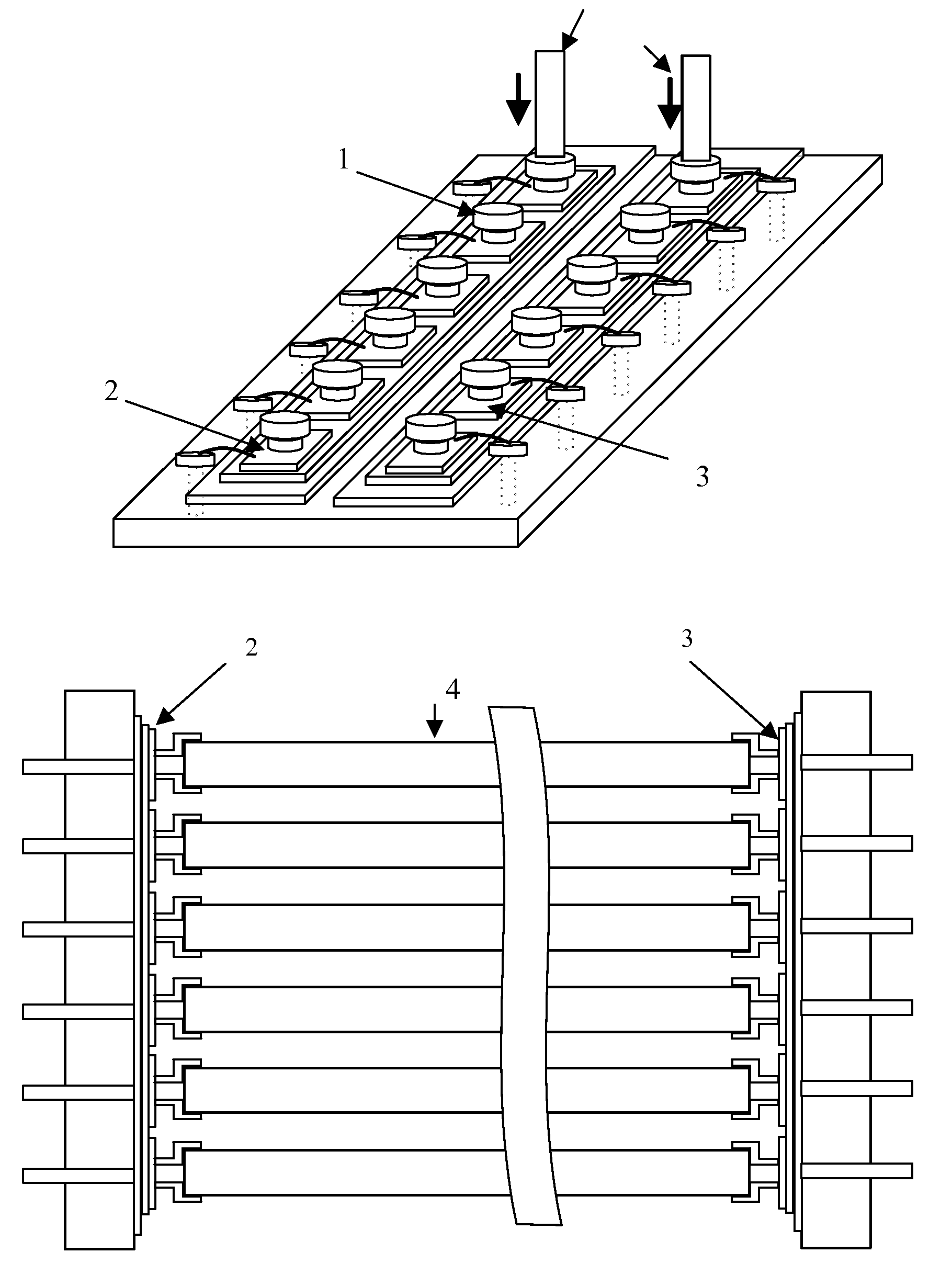
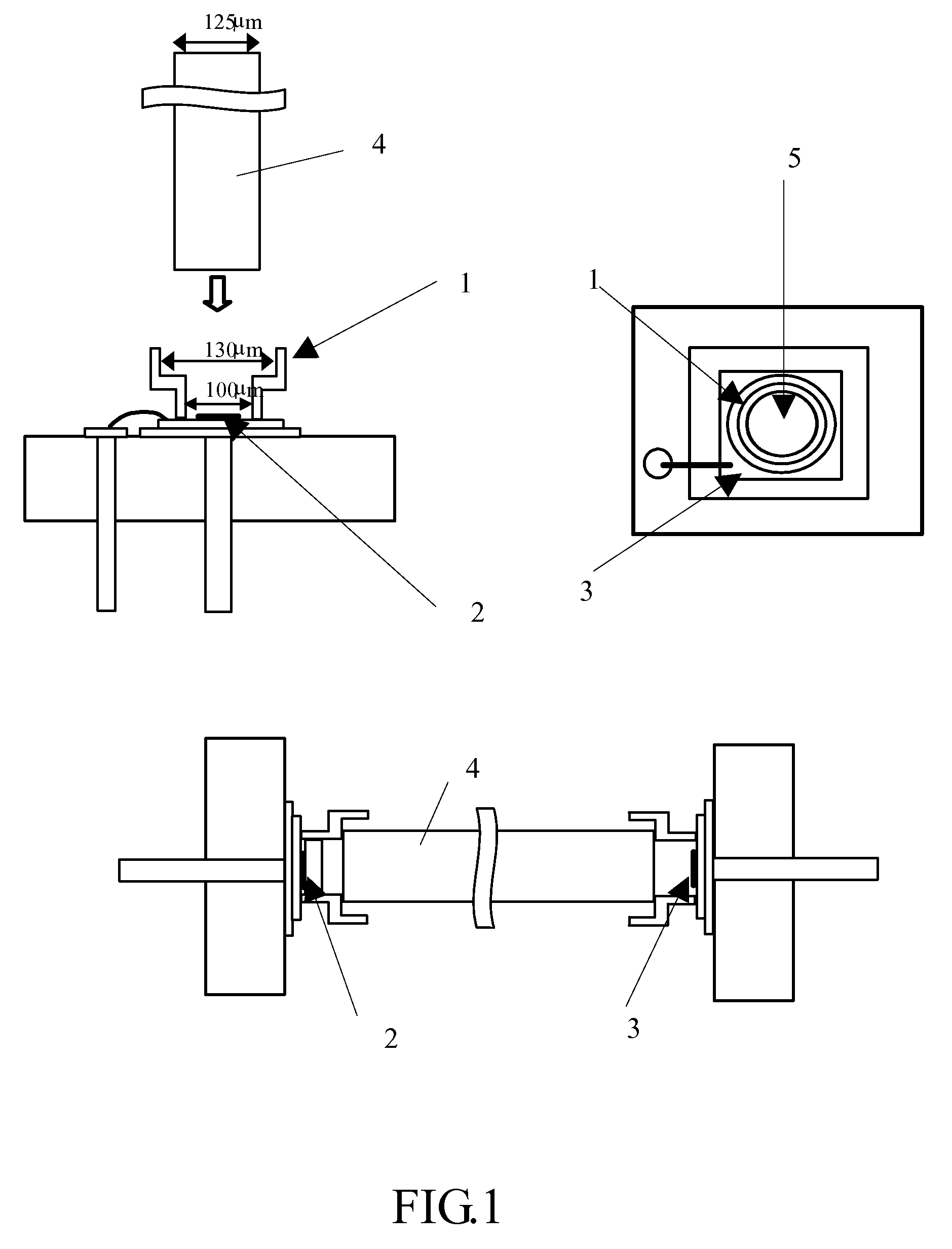
[0022]Referring to FIG. 1 and taking one of the wafers in the array as example, the integrated circuit having compact high-speed optical signal bus lines of the present invention comprises:

[0023]a Multi-mode optical fiber, in which two ends of the multi-mode optical fiber are placed in the fiber holes 1, respectively;

[0024]a Vertical Cavity Surface Emitting Laser Array (VCSEL Array) 2 with the fiber holes 1 in which the light source for VCSEL Array 2 can be LED or other surface emitting lasers;

[0025]a PIN Array 3 with the fiber holes 1 wherein the material of PIN Array is silicon; and

[0026]a Multi-mode optical fiber 4 with optical core having great diameter.

[0027]Referring to VCSEL Array 2 that has the fiber holes 1 and PIN Array 3 having the fiber holes 1 wherein the fiber holes 1 are formed in VCSEL light emitting area / PIN light receiving area 5, respectively, by microelectromechanical system (MEMC) technology as a concentric cylinder shape with diameter 100 μm, height 30 μm and d...


PUM


Abstract

An integrated circuit having compact high-speed bus lines consists of VCSEL Array providing optical fiber holes, PIN Array providing optical fiber holes, and multi-mode optical fiber with great diameter optical core, wherein the VCSEL Array providing optical fiber holes and the PIN Array providing optical fiber holes both utilize the microelectromechanical system (MEMC) technology to form optical fiber holes as a concentric cylinder shape with diameter 100 μm, height 30 μm and diameter 130 μm, height 80-100 μm in the VCSEL light emitting area and the PIN light receiving area, respectively. An integrated package can be easily accomplished by mechanically performing focusing package of fixed optic-insertion to complete a glued integrated package, and thereby the package cost as a majority of the prime cost can be greatly reduced.

Description

BACKGROUND OF THE INVENTION[0001]1. Field of the Invention[0002]The present invention is related to an integrated circuit having compact high-speed bus lines for optical signals to be used in ultra-speed electronic circuit boards and its interface connections. The present invention is adaptable for different electric connectors and used for optical signal transmissions between interface ICs of high-speed routers and switches for linking up a high-speed bus.[0003]2. Description of the Prior Art[0004]Due to strong demand of high-speed broadband, a design of preventing interferences incurred by transmitting broadband signals between high-density copper wires has become difficult. The existing apparatuses for optical signal interconnecting are complex and cause high manufacturing cost than average electronic products, thus which cannot be efficiently utilized. Most of the short distance optical signal connections that employed point-to-point optical interface connections which is diffic...

Claims


Application Information

Patent Timeline
IPC IPC(8): G02B6/12
CPCG02B6/4202G02B6/4249
Inventor LIAO, HUNG-HUEIHO, CHONG-LONG
Owner CHUNGHWA TELECOM CO LTD
Why Eureka
Try Eureka