Contactor nest for an IC device and method

Active Publication Date: 2008-10-30
ESSAI INC
View PDF8 Cites 7 Cited by
  • Summary
  • Abstract
  • Description
  • Claims
  • Application Information

AI Technical Summary

Benefits of technology

[0012]Therefore, it can be seen that it is a primary object of the present invention to provide an improved contactor nest and method that reduces the risk of jamming as the IC device under test is inserted into and removed from a test contactor. It is a further object of the inven

Problems solved by technology

However, the difficulty with such contactor nest designs is that DUTs frequently jam as they are passed through the straight-walled guide section of the contactor nest pocket due to the tight tolerance involved and mismatches caused by out-of-tolerance DUTs and thermal expansion.
Jamming leads to frequent “drop-outs” of DUTs during high volume testing.
Another problem enco

Method used


Image

  • Contactor nest for an IC device and method
  • Contactor nest for an IC device and method
  • Contactor nest for an IC device and method

Examples


Example

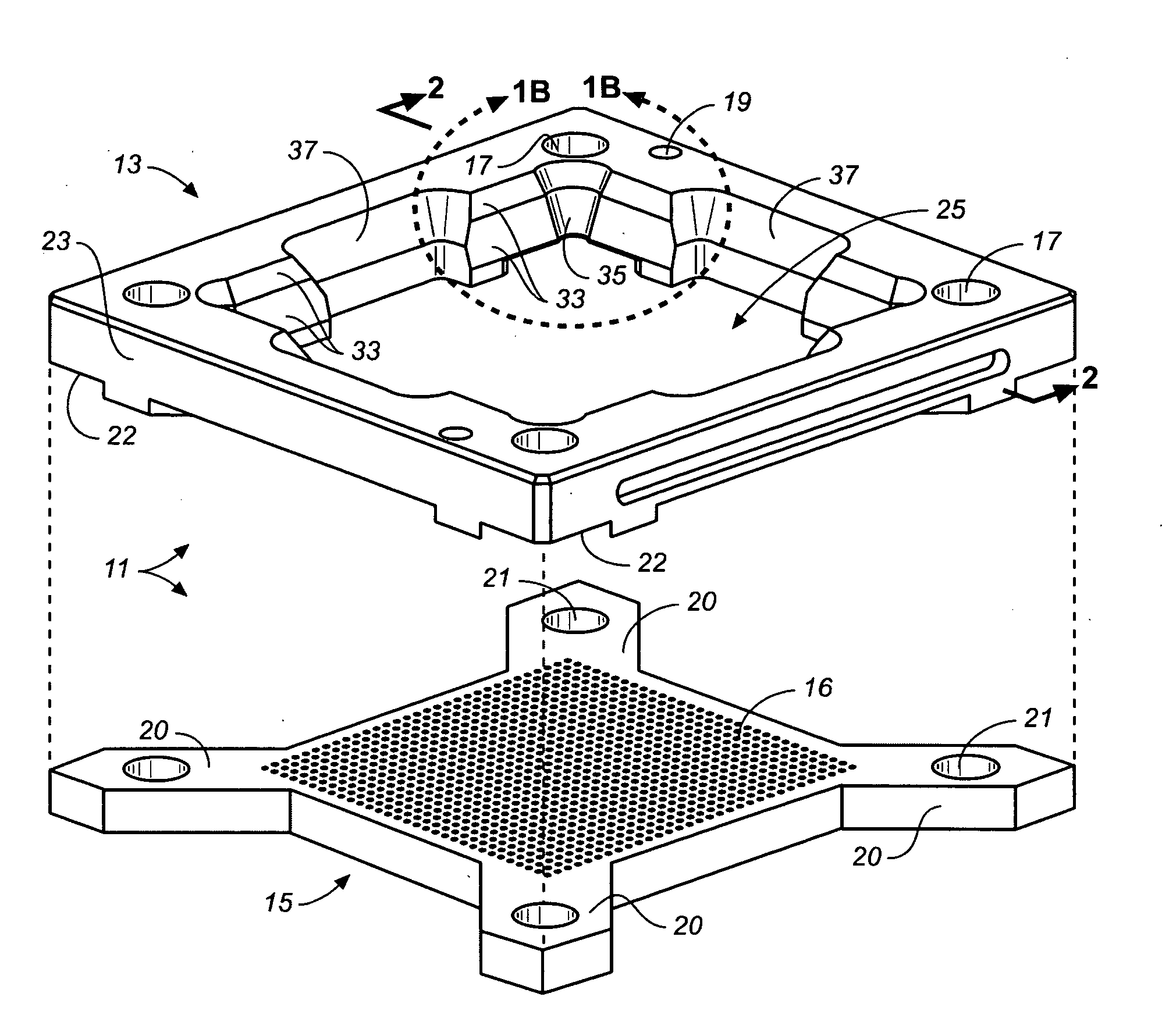
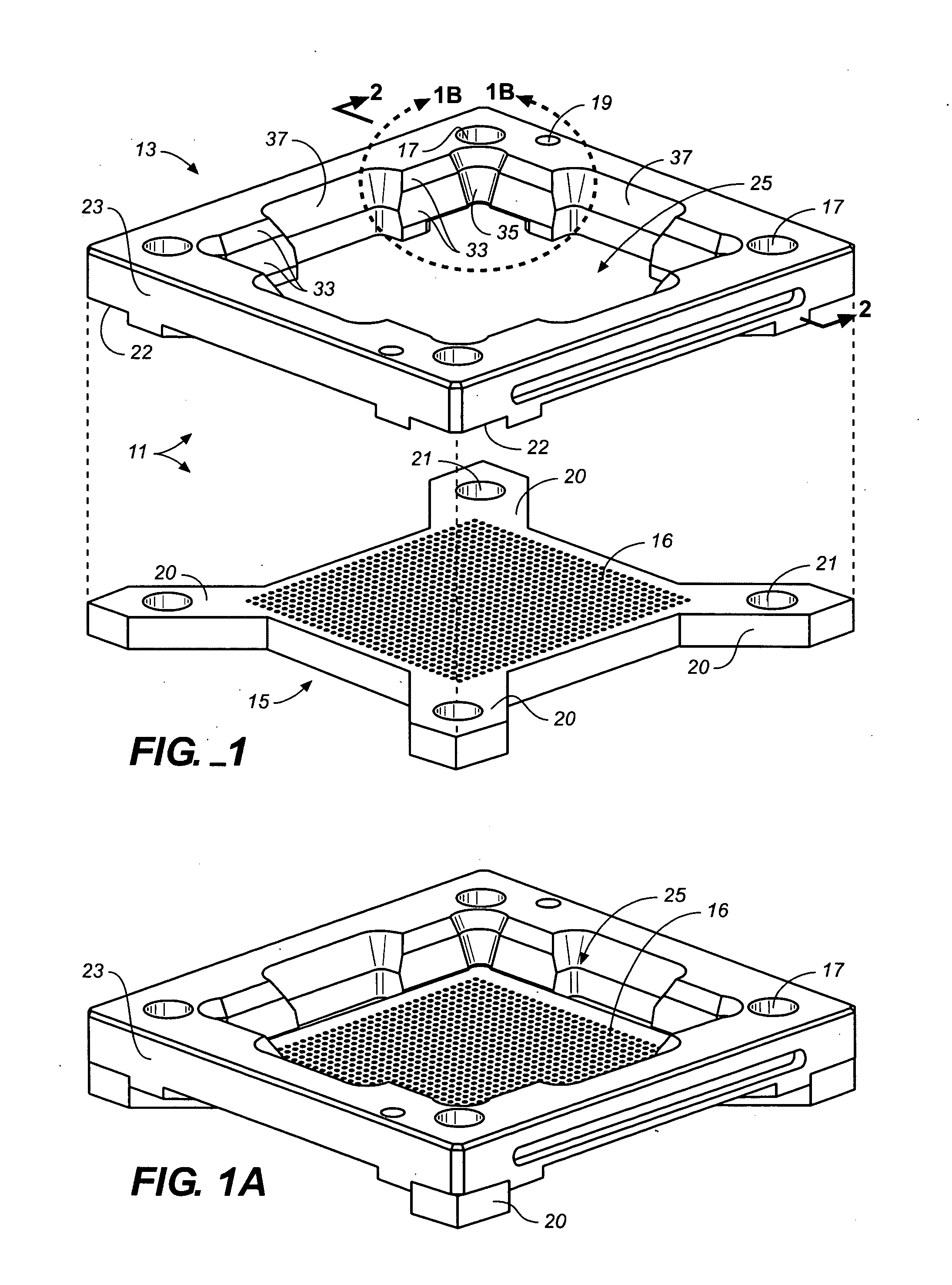
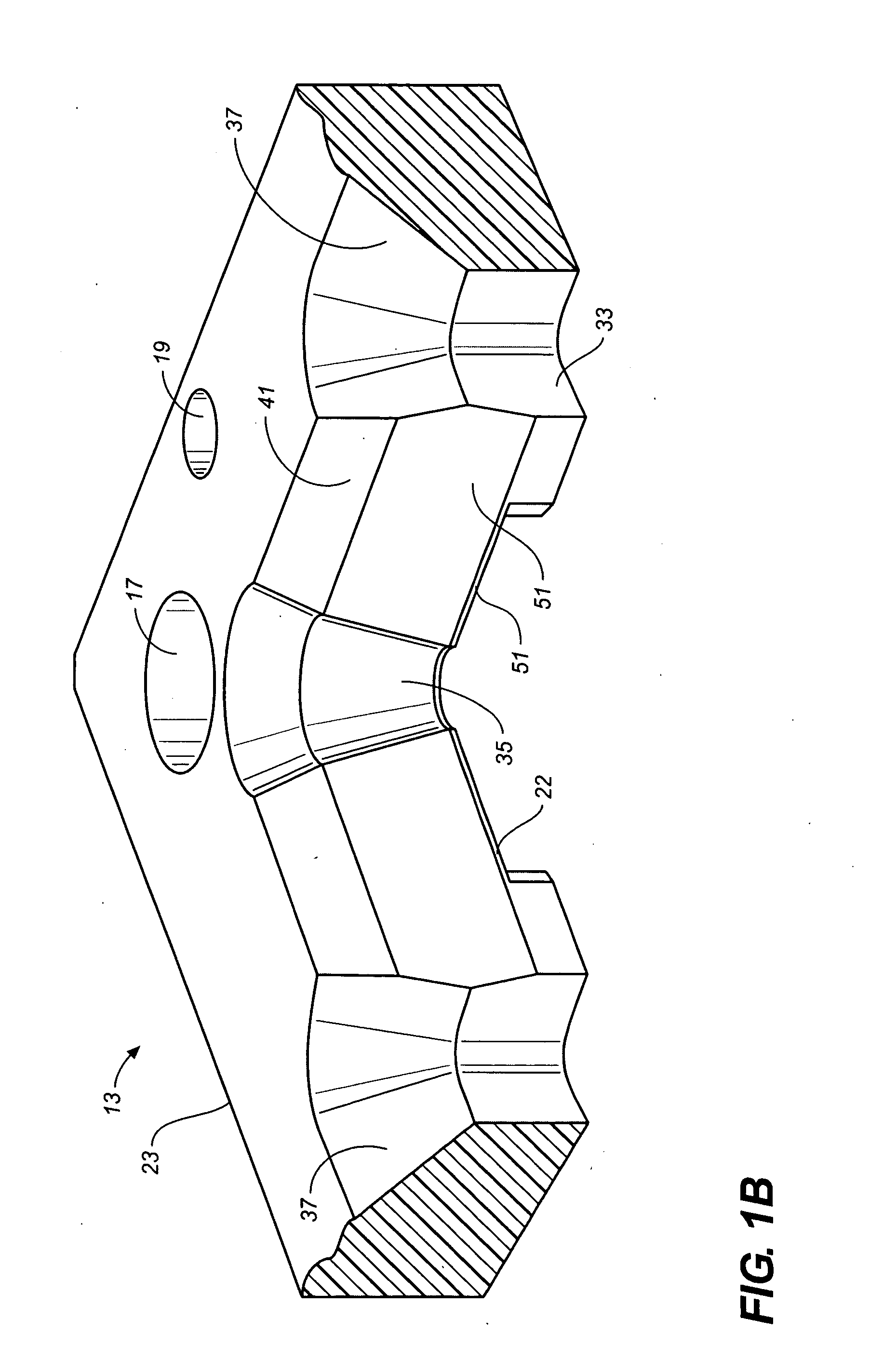
[0020]Referring now to the drawings, a test contactor 11 is comprised of a contactor nest 13 and a pin board interposer 15, which together are mounted by a load board (not shown) by suitable fasteners (not shown) inserted through fastener openings 17 and 19 in the contactor nest and the fastener openings 21 in the interposer's corner arms 20, which fit into corner recesses 22 on the underside the perimeter frame 23 of the contactor nest. In addition to perimeter frame 23, the contactor nest has a central IC device pocket 25 sized to receive and capture an IC device having a given footprint. When the contactor nest and pin board interposer are mounted together on a load board, the contactor nest will function to guide the IC device onto the pin board interposer and align the IC device with the interposer pins as hereinafter described. IC devices will typically be inserted into and removed from the contactor nest by automated chip handling equipment which are well known in the art.

[00...


PUM


Abstract

An improved contactor nest for receiving and holding IC devices against a pin board interposer during the test or burn-in of the devices includes a frame having an IC pocket with a top opening, which is oversized in relation to the footprint of the IC device for which the contactor is designed, and centering guide walls for guiding an IC device to be tested into the pocket from the oversized top opening to the IC device seating plane. The centering guide walls have a gradual angle relative to the insertion axis of the IC pocket, and extend down to a bottom perimeter portion of the IC pocket immediately adjacent the IC seating plane for gradually centering the IC device in the pocket as the IC device approaches the seating plane. Preferably, the angled guide walls extend far enough into the IC pocket to allow the spring pins of the pin board interposer to scrub the contact pads of the IC devices as the IC device is being centered.

Description

CROSS-REFERENCED TO RELATED APPLICATIONS[0001]This application claims the benefit of U.S. Provisional Application No. 60 / 753,825 filed Dec. 23, 2005.BACKGROUND OF THE INVENTION[0002]The present invention generally relates to test contactors used to establish an electrical interface between an integrated circuit (IC) device under test and a circuit board, and, more particularly, relates to contactor nests used to guide an IC device into contact with an array of contact pins of an interposer that electrically interfaces with a circuit board.[0003]Contactors are widely used to hold IC devices onto a test or load board for test or burn-in. Such contactors typically include an interposer and contactor nest. The interposer, which contains an array of conductors that match up with the I / O contact pads on the device under test (DUT), provides an electrical interface between the DUT and the test board. The contactor nest guides the DUT onto the interposer. The interposer can be integral part...

Claims


Application Information

Patent Timeline
IPC IPC(8): G01R1/02
CPCG01R1/0466G01R1/0483
Inventor BARABI, NASSERKRYACHEK, OKSANAHO, CHEE-WAH
Owner ESSAI INC
Why Eureka
Try Eureka