Light emitting optical film and manufacture method thereof and liquid crystal display device

Inactive Publication Date: 2008-10-30
TAIWAN TFT LCD ASSOC +6
View PDF15 Cites 5 Cited by
  • Summary
  • Abstract
  • Description
  • Claims
  • Application Information

AI Technical Summary

Benefits of technology

[0012]The present invention further provides an LCD device, which includes a liquid crystal panel and a light emitting source. The liquid crystal panel at least includes a means constituted by a second alignment layer and a polarized light emitting liquid crystal film, and the polarized light emitting liquid crystal film includes liquid crystal and light-emitting dye. The light emitting source is located on any side of the liquid crystal panel, and lights emitted by the light emitting source can enable the polarized light emitting liquid crystal film to emit lights at wavelength scope different from that of the lights emitted by the light emitting source.
[0013]In the present invention, the liquid crystal material alignment function is utilized together

Problems solved by technology

As for the manufacturing process and design of a conventional optical film used by a display device, the manufacturing process is complex and the cost is high.
The manufacturing process not only restricts the materials and functions, but also redundant substrate causes the over-high material cost, directly or indirectly affects the optical characteristics, and further results in

Method used


Image

  • Light emitting optical film and manufacture method thereof and liquid crystal display device
  • Light emitting optical film and manufacture method thereof and liquid crystal display device
  • Light emitting optical film and manufacture method thereof and liquid crystal display device

Examples


first embodiment

The First Embodiment

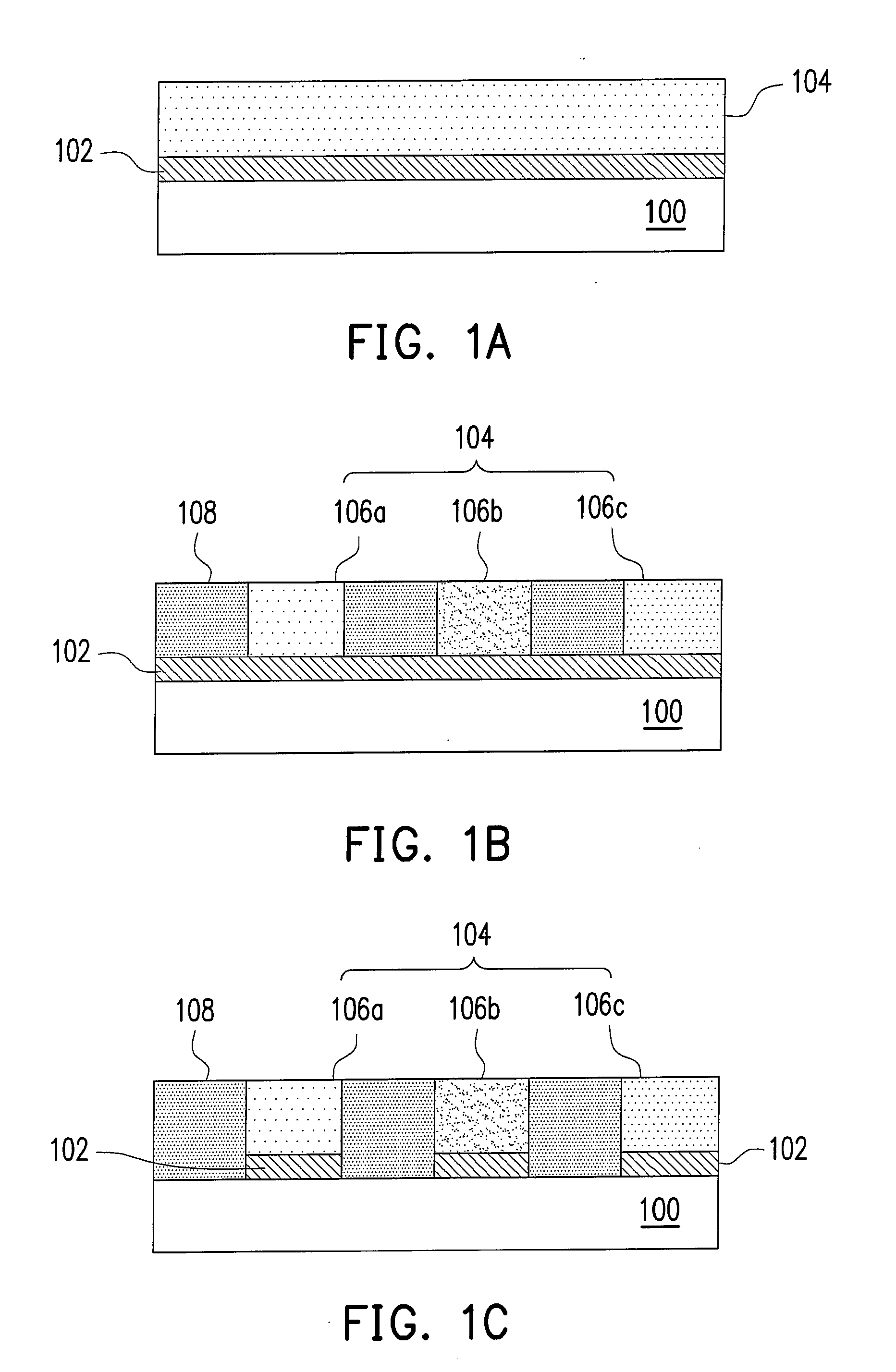
[0025]FIGS. 1A to 1C are respectively sectional views of three structural variations of a light emitting optical film according to a first embodiment of the present invention.

[0026]Firstly, referring to FIG. 1A, a first light emitting optical film includes a substrate 100, an alignment layer 102, and a polarized light emitting liquid crystal film 104. The polarized light emitting liquid crystal film 104 includes liquid crystal and light-emitting dye. The liquid crystal is, for example, liquid crystal polymer, liquid crystal oligomer, or liquid crystal monomer. The light-emitting dye is organic light-emitting diode (OLED)-like dyes, for example, dichroic dyes. The polarized light emitting liquid crystal film 104 can change the color of the light according to different wavelength characteristics of different light-emitting dyes. The substrate 100 can be a light-transmissive substrate or an opaque substrate.

[0027]Referring to FIG. 1A, the alignment layer 102 is loca...

second embodiment

The Second Embodiment

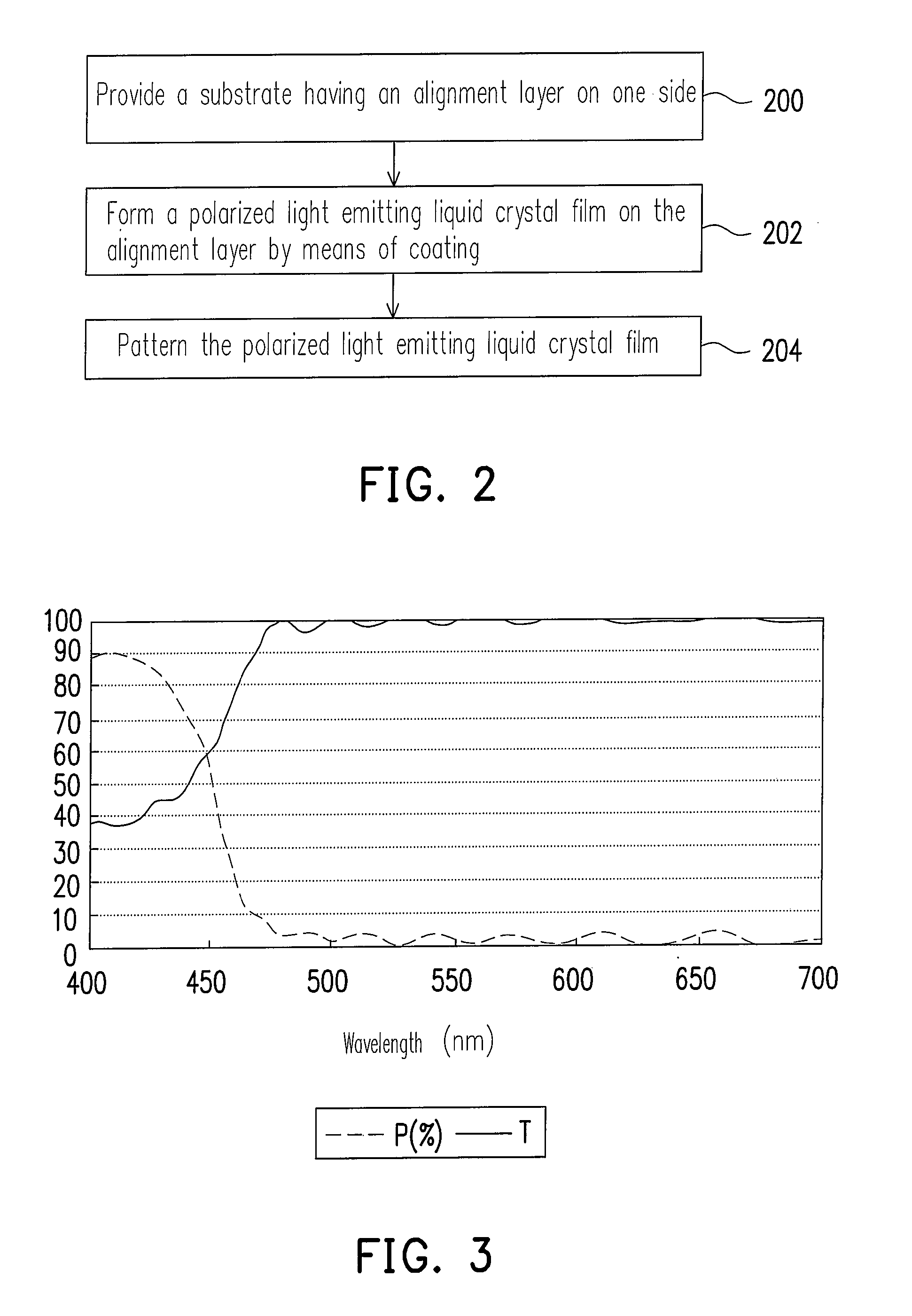
[0030]FIG. 2 is a flow chart for manufacturing a light emitting optical film according to a second embodiment of the present invention.

[0031]Referring to FIG. 2, in Step 200, a substrate is provided, which is a light-transmissive substrate or an opaque substrate. The substrate has an alignment layer on one side.

[0032]Next, in Step 102, a polarized light emitting liquid crystal film is formed on the alignment layer by means of coating, and the polarized light emitting liquid crystal film is at least formed by liquid crystal or light-emitting dye. The material of the polarized light emitting liquid crystal film is formed by dissolving the light-emitting dye in the liquid crystal, by utilizing the different light-emitting dyes absorption and the light emitting effects together with the liquid crystal combination, it is applied to optical films with different functions, such as a polarizing film capable of emitting the polarized light or a phase retardation film cap...

third embodiment

The Third Embodiment

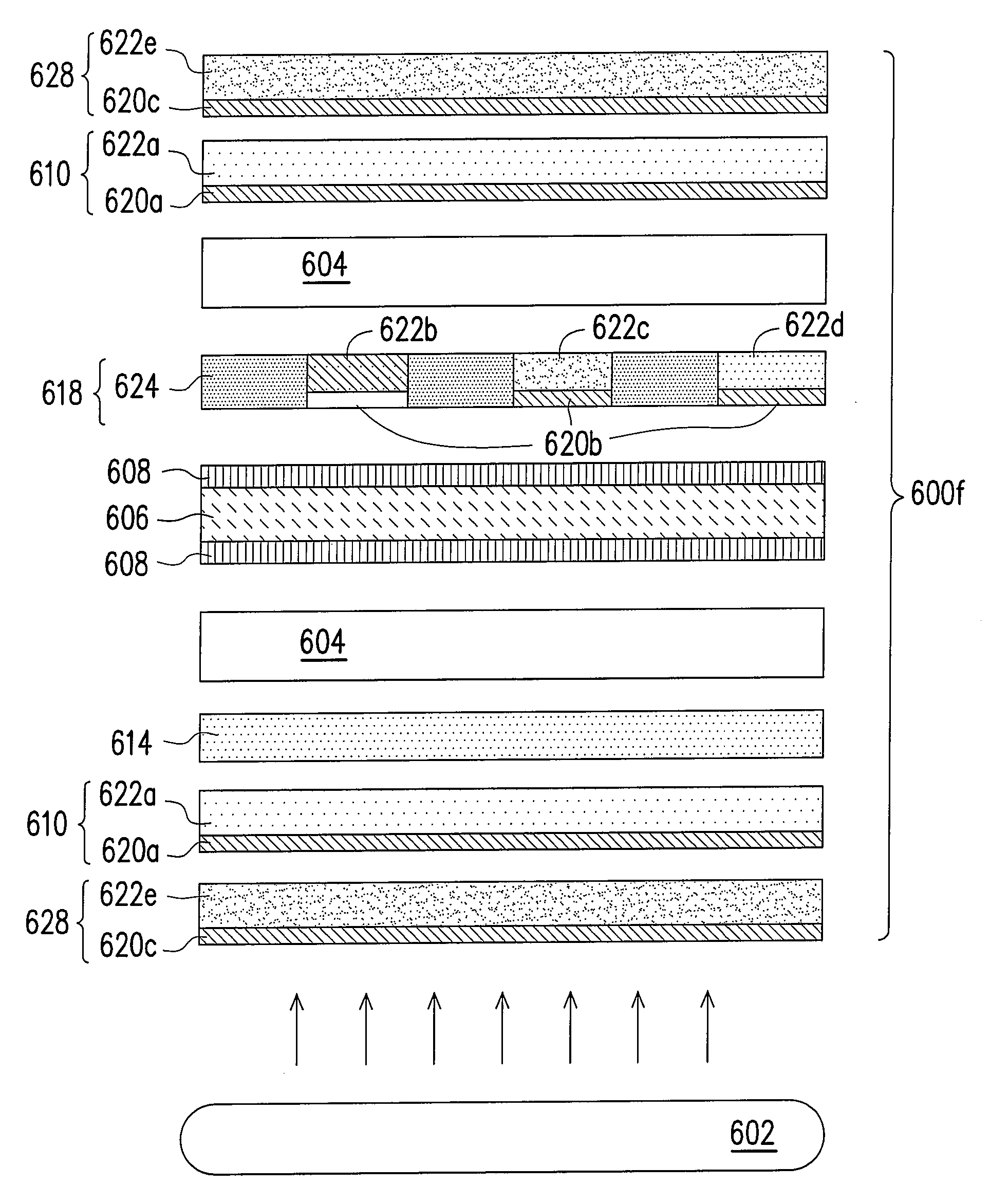
[0037]The LCD device of the third embodiment mainly includes a liquid crystal panel and a light emitting source. The liquid crystal panel at least includes one means constituted by a second alignment layer and a polarized light emitting liquid crystal film, and the polarized light emitting liquid crystal film includes liquid crystal and light-emitting dye. The light emitting source is located on any side of the liquid crystal panel, and the lights emitted by the light emitting source can enable the polarized light emitting liquid crystal film to emit lights with wavelength scope different from that of the lights emitted by the light emitting source. The sectional exploded views of several structures thereof are described below.

[0038]Firstly, referring to FIG. 6A, the LCD device of this embodiment includes a liquid crystal panel 600a and a light emitting source 602. The liquid crystal panel 600a includes two electrode substrates 604, a liquid crystal layer 606 san...


PUM


Abstract

A light emitting optical film at least including a substrate, an alignment layer and a polarized light emitting liquid crystal film is provided, in which the polarized light emitting liquid crystal film includes liquid crystal and light-emitting dye. The alignment layer is located on one side of the substrate, and the polarized light emitting liquid crystal film is located on the alignment layer. The light emitting optical film can be applied to polarizing film, phase retardation film or color filter. Moreover, it is unnecessary to use conventional backlight module because overall arrangement of liquid crystal can fully emit uniform polarized light, whereby greatly reducing cost of conventional backlight module.

Description

CROSS-REFERENCE TO RELATED APPLICATION[0001]This application claims the priority benefit of Taiwan application serial no. 96115251, filed on Apr. 30, 2007. All disclosure of the Taiwan application is incorporated herein by reference.BACKGROUND OF THE INVENTION[0002]1. Field of the Invention[0003]The present invention relates to a light emitting optical film, a manufacture method thereof, and a liquid crystal display (LCD) device.[0004]2. Description of Related Art[0005]As for the manufacturing process and design of a conventional optical film used by a display device, the manufacturing process is complex and the cost is high. Furthermore, a substrate layer is required for support or protection, so as to finish the manufacturing process and the design of the optical film. The optical film is mainly used through adhering. The manufacturing process not only restricts the materials and functions, but also redundant substrate causes the over-high material cost, directly or indirectly aff...

Claims


Application Information

Patent Timeline
IPC IPC(8): G02F1/13357G02F1/13
CPCG02F1/133621G02F1/13475G02F1/13725G02F2202/04
Inventor JENG, YUE-SHIHYANG, KEI-HSIUNG
Owner TAIWAN TFT LCD ASSOC
Why Eureka
Try Eureka