Non-volatile memory and manufacturing method and operating method thereof and circuit system including the non-volatile memory

a manufacturing method and non-volatile memory technology, applied in the field of semiconductor devices, can solve the problems of increasing the manufacturing cost, occupying a lot of space, and prolonging the manufacturing process, so as to improve the reliability of the memory cell and the electrical performance of the memory, and facilitate programming, erased and read.

Active Publication Date: 2008-10-30
MACRONIX INT CO LTD
View PDF3 Cites 135 Cited by
  • Summary
  • Abstract
  • Description
  • Claims
  • Application Information

AI Technical Summary

Benefits of technology

[0060]Moreover, since the charge trapping layers in such a memory cell are respectively disposed at two sides of the gates, the various bits can be easily programmed, erased, and read by supplying appropriate voltages to t...

Problems solved by technology

Thus, a plurality of mask processes has to be performed during the fabricating process, which not only prolongs the fabricating process but also increases the fabricating cost.
Moreover, a memory cell in the EEPROM can only store a 1-bit data and the double-gate design also takes a lot of sp...

Method used


Image

  • Non-volatile memory and manufacturing method and operating method thereof and circuit system including the non-volatile memory
  • Non-volatile memory and manufacturing method and operating method thereof and circuit system including the non-volatile memory
  • Non-volatile memory and manufacturing method and operating method thereof and circuit system including the non-volatile memory

Examples


Embodiment Construction

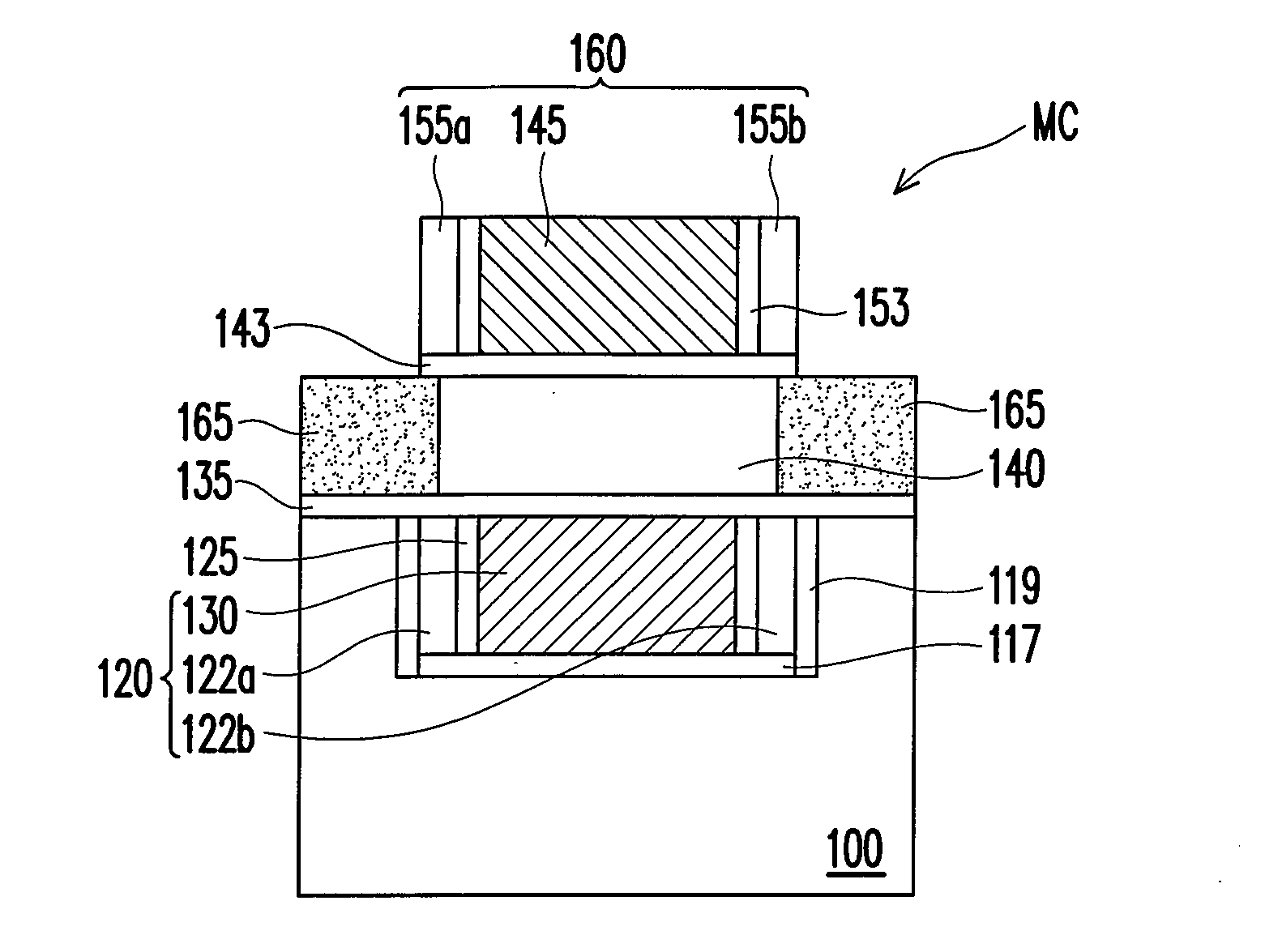
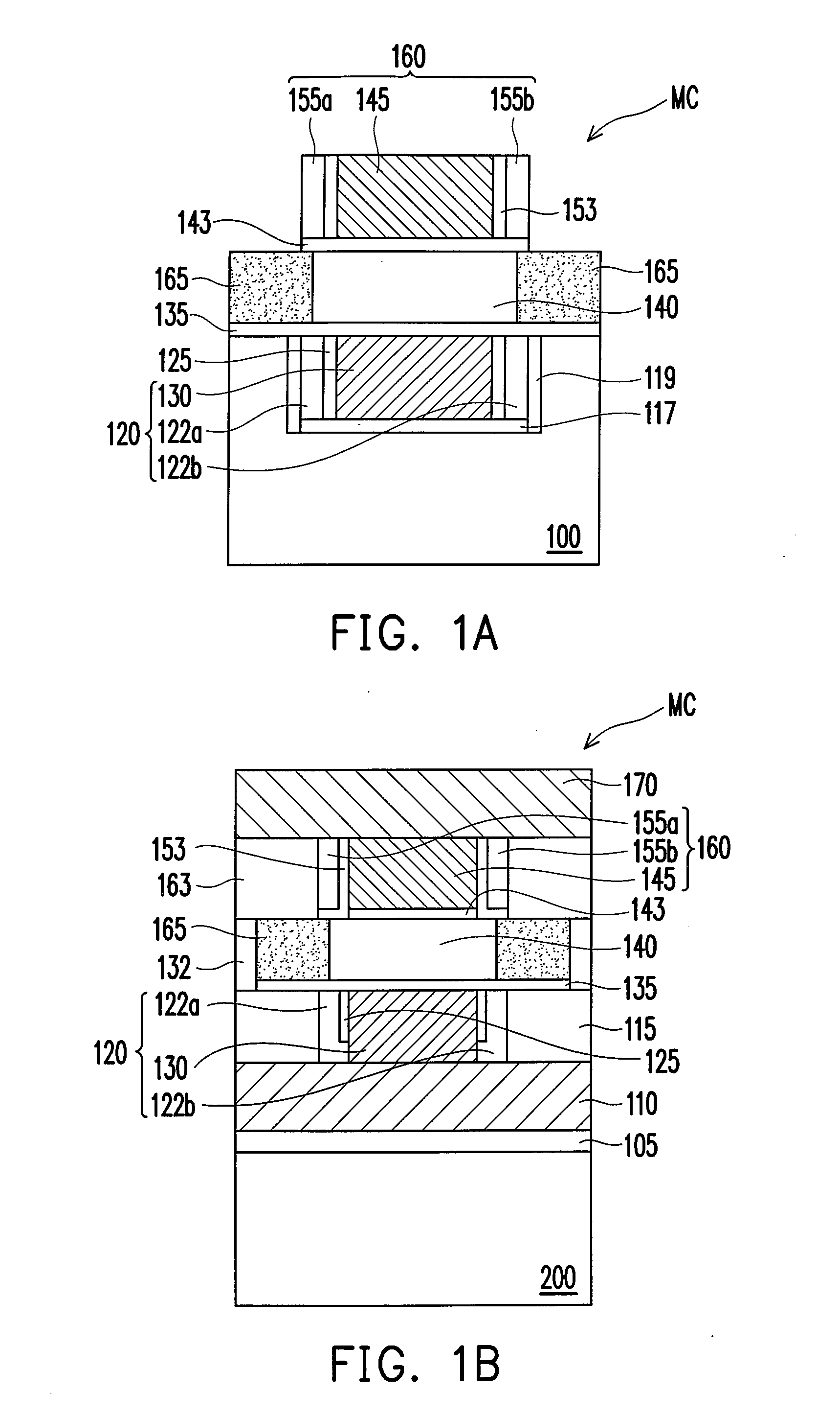
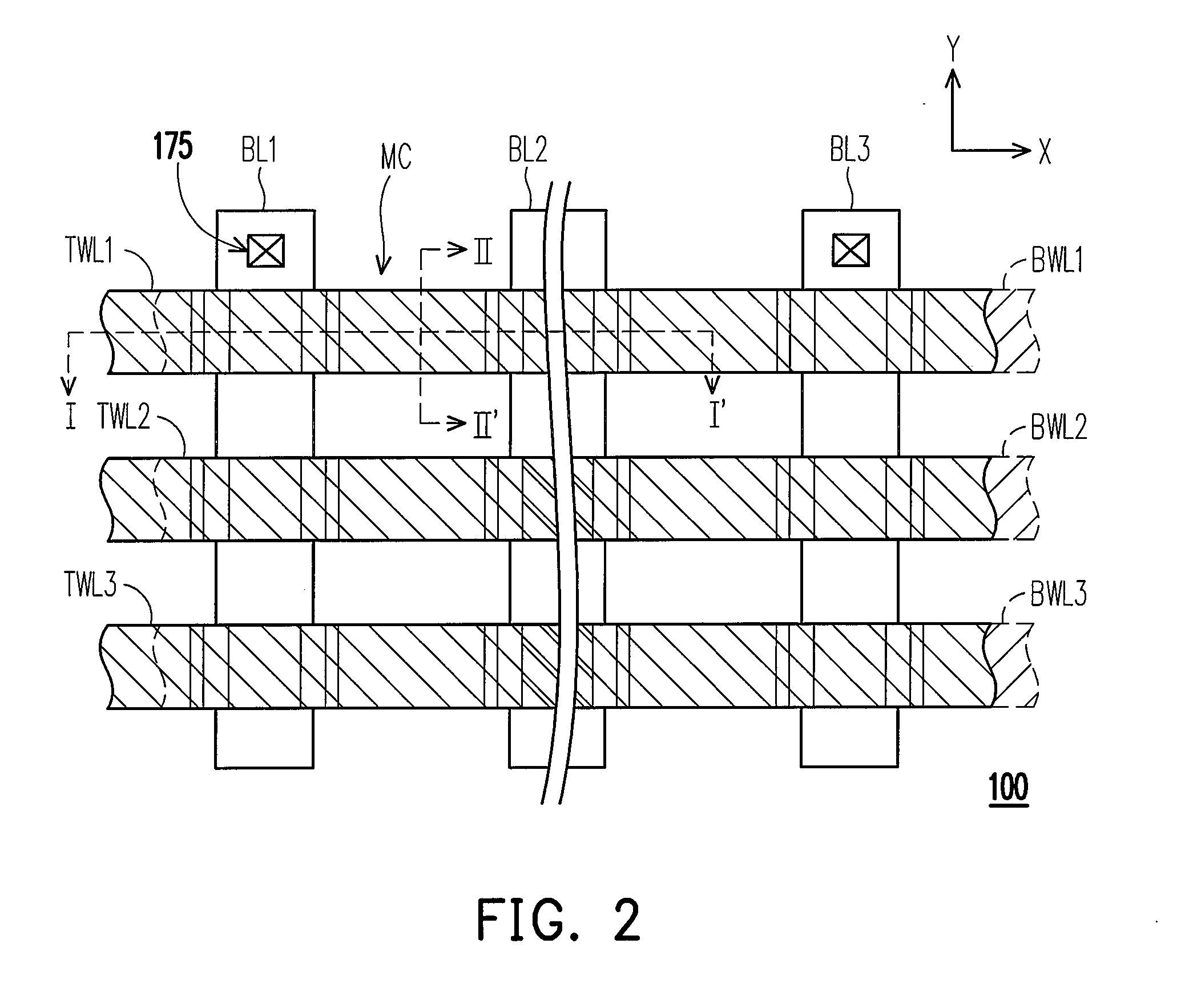
[0074]FIG. 1A is a cross-sectional view of a non-volatile memory according to an embodiment of the present invention. FIG. 1B is a cross-sectional view of a non-volatile memory according to another embodiment of the present invention. FIG. 2 is a top view of a non-volatile memory according to an embodiment of the present invention.

[0075]Referring to FIG. 1A and FIG. 1B, a single memory cell MC is used for describing the non-volatile memory in the present invention. The memory cell MC is disposed on a substrate 100 and is composed of a semiconductor layer 140, a first unit 120, a second unit 160, and a doped region 165.

[0076]Referring to FIG. 1A, the substrate 100 may be a silicon substrate. The first unit 120 includes a first gate 130, and a first charge trapping layer 122a and a second charge trapping layer 122b disposed at both sides of the first gate 130. The material of the first gate 130 may be doped polysilicon, and the material of the first charge trapping layer 122a and the ...


PUM


Abstract

A non-volatile memory including a memory cell is described. The memory cell includes a first unit, a semiconductor layer, a second unit, and a doped region. The first unit includes a first gate, a first charge trapping layer, and a second charge trapping layer. The first and the second charge trapping layer are respectively disposed on both sides of the first gate. The semiconductor layer is disposed on the first unit. The second unit is disposed on the semiconductor layer and is in mirror symmetry to the first unit. The second unit includes a second gate and a third and a fourth charge trapping layer respectively disposed on both sides of the second gate. The doped region is disposed at both sides of the semiconductor layer and serves as a common source/drain region of both the first and the second unit.

Description

BACKGROUND OF THE INVENTION[0001]1. Field of the Invention[0002]The present invention relates to a semiconductor device and a manufacturing method and an operating method thereof. More particularly, the present invention relates to a non-volatile memory and a manufacturing method and an operating method thereof.[0003]2. Description of Related Art[0004]Data can be written into and read or erased from an electrically erasable programmable read-only memory (EEPROM) repeatedly and the data stored in the EEPROM won't be lost even after the power is cut off. Thus, EEPRM among non-volatile memories has been broadly applied to personal computers and electronic equipments.[0005]Typically, the floating gate and control gate of an EEPROM are fabricated with doped polysilicon, and the insulation layers between gates and the substrate and between gate and gate are silicon oxide layers.[0006]However, a plurality of polysilicon layers and a plurality of silicon oxide layers are to be formed in the...

Claims


Application Information

Patent Timeline
IPC IPC(8): G11C11/34H01L21/336H01L29/76
CPCH01L21/28282H01L29/42348H01L29/66833H01L29/7923H01L29/40117
Inventor KUO, MING-CHANG
Owner MACRONIX INT CO LTD
Why Eureka
Try Eureka