Methods for conducting double-side-biasing operations of NAND memory arrays

Active Publication Date: 2008-10-30
MACRONIX INT CO LTD
View PDF5 Cites 18 Cited by
  • Summary
  • Abstract
  • Description
  • Claims
  • Application Information

AI Technical Summary

Benefits of technology

[0014]Advantageously, the double-side-bias electron injection method emulates a pl

Problems solved by technology

However, the hot hole injection causes oxide damage, leading to charge loss in the high threshold cell and charge gain in the low threshold cell.
This difference in erase speed results in a large Vt distribution of the erase state, where some of the cells be

Method used


Image

  • Methods for conducting double-side-biasing operations of NAND memory arrays
  • Methods for conducting double-side-biasing operations of NAND memory arrays
  • Methods for conducting double-side-biasing operations of NAND memory arrays

Examples


Embodiment Construction

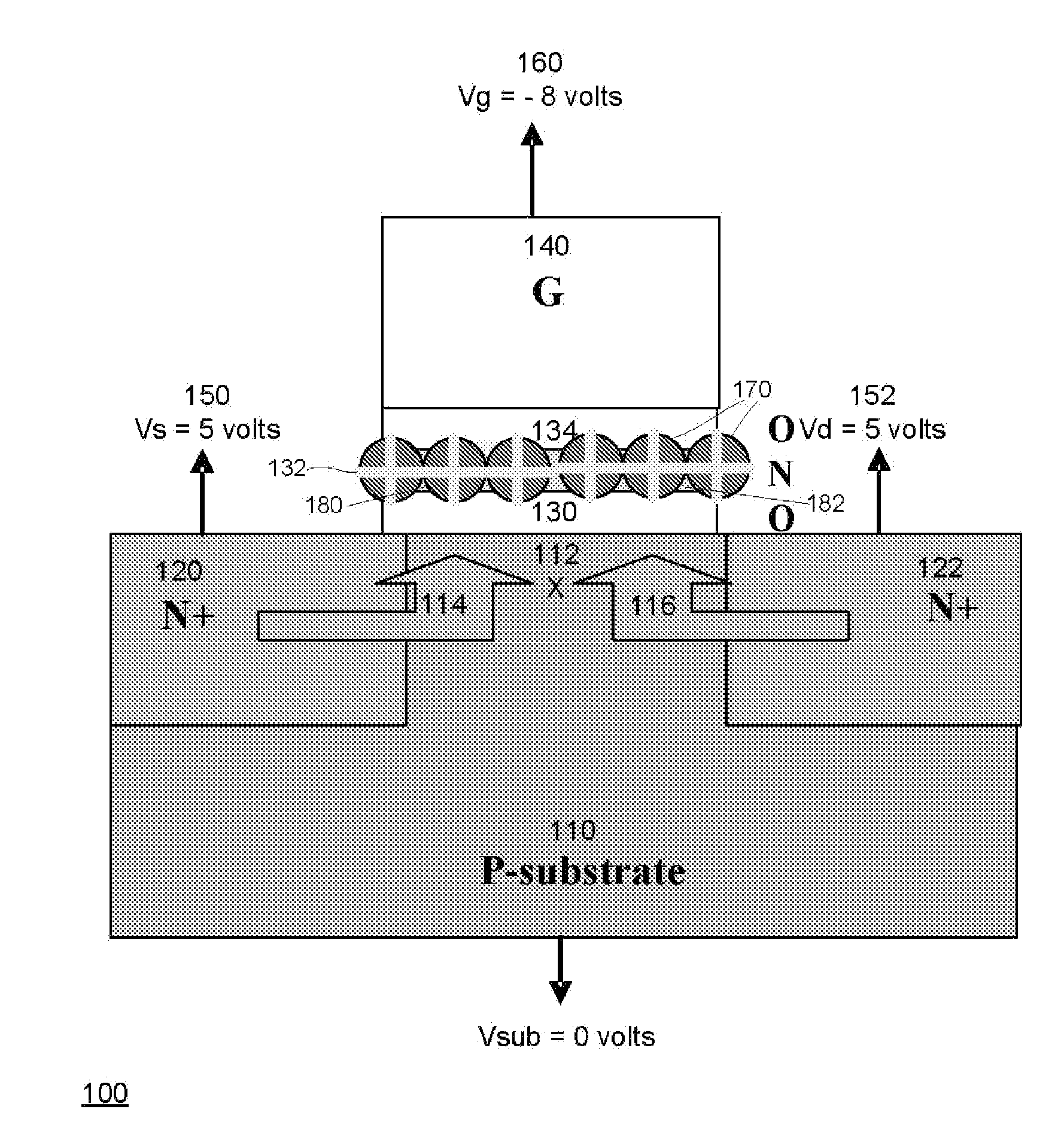
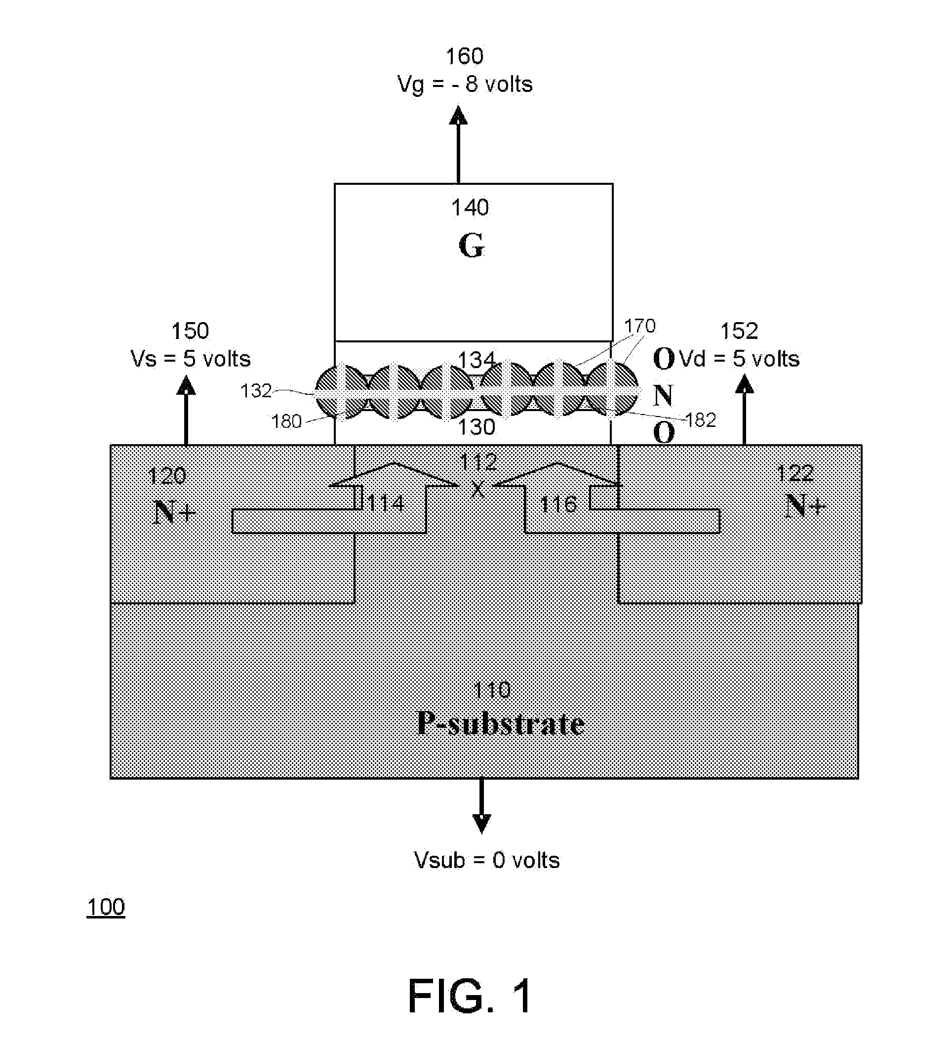
[0030]A description of structural embodiments and methods of the present invention is provided with reference to FIGS. 1-13. It is to be understood that there is no intention of limiting the invention to the specifically disclosed embodiments. Rather, the invention may be practiced using other features, elements, methods and embodiments. Like elements in various embodiments are commonly referred to with like reference numerals.

[0031]FIG. 1 is a process diagram illustrating a cross-sectional view of erasing a charge trapping memory cell (or N-bit) 100 by a double-side-bias (DSB) hole injection (HI) method. The charge trapping memory cell 100 comprises a p-substrate 110 with n+ doped regions 120 and 122, and a p-doped region between the n+ doped regions 120 and 122. A first directional flow 114 indicates the flow of hole charges from the n+ doped region 120, and a second directional flow 116 indicates the flow of hole charges from the n+ doped region 122. A channel width X 112 of the ...


PUM


Abstract

Methods are described for double-side-biasing of a NAND memory array device comprising a plurality of charge trapping memory cells for programming and erasing the NAND memory array device. A double-side-biasing method applies a bias voltage simultaneously on a first junction (a source region) and a second junction (a drain region) so that a left bit and a right bit in a charge trapping memory cell can be programmed in parallel or erased in parallel. Random (or selective) bit program and random (or selective) bit erase can be achieved by using a double-side-biasing method on a NAND memory array device for both data and code application. A first type of double-side-biasing method is to program the NAND array with a double-side-bias electron injection. A second type of double-side-biasing method is to erase the NAND array with a double-side-bias hole injection.

Description

BACKGROUND OF THE INVENTION[0001]1. Field of the Invention[0002]The present invention relates generally to electrically programmable and erasable memory and more particularly to charge storage devices for monitoring charging effect.[0003]2. Description of Related Art[0004]Electrically programmable and erasable nonvolatile memory technologies based on charge storage structures known as Electrically Erasable Programmable Read-Only Memory (EEPROM) and flash memory are used in a variety of modern applications. A flash memory is designed with an array of memory cells that can be independently programmed and read. Sense amplifiers in a flash memory are used to determine the data value or values stored in a nonvolatile memory. In a typical sensing scheme, an electrical current through the memory cell being sensed is compared to a reference current by a current sense amplifier.[0005]A number of memory cell structures are used for EEPROM and flash memory. As the dimensions of integrated circ...

Claims


Application Information

Patent Timeline
IPC IPC(8): G11C11/34
CPCG11C16/0475G11C16/0483G11C16/10
Inventor WU, CHAO-I
Owner MACRONIX INT CO LTD
Why Eureka
Try Eureka