
Memory Redundancy Method and Apparatus

Inactive Publication Date: 2008-10-30
QIMONDA
View PDF5 Cites 11 Cited by
  • Summary
  • Abstract
  • Description
  • Claims
  • Application Information

AI Technical Summary

Problems solved by technology

A single failing memory cell amongst millions in a memory device causes failure.
However, redundant word lines conventionally have a width matching the widest data bus organization available for a particular memory device.

Method used


Image

  • Memory Redundancy Method and Apparatus
  • Memory Redundancy Method and Apparatus
  • Memory Redundancy Method and Apparatus

Examples


Embodiment Construction

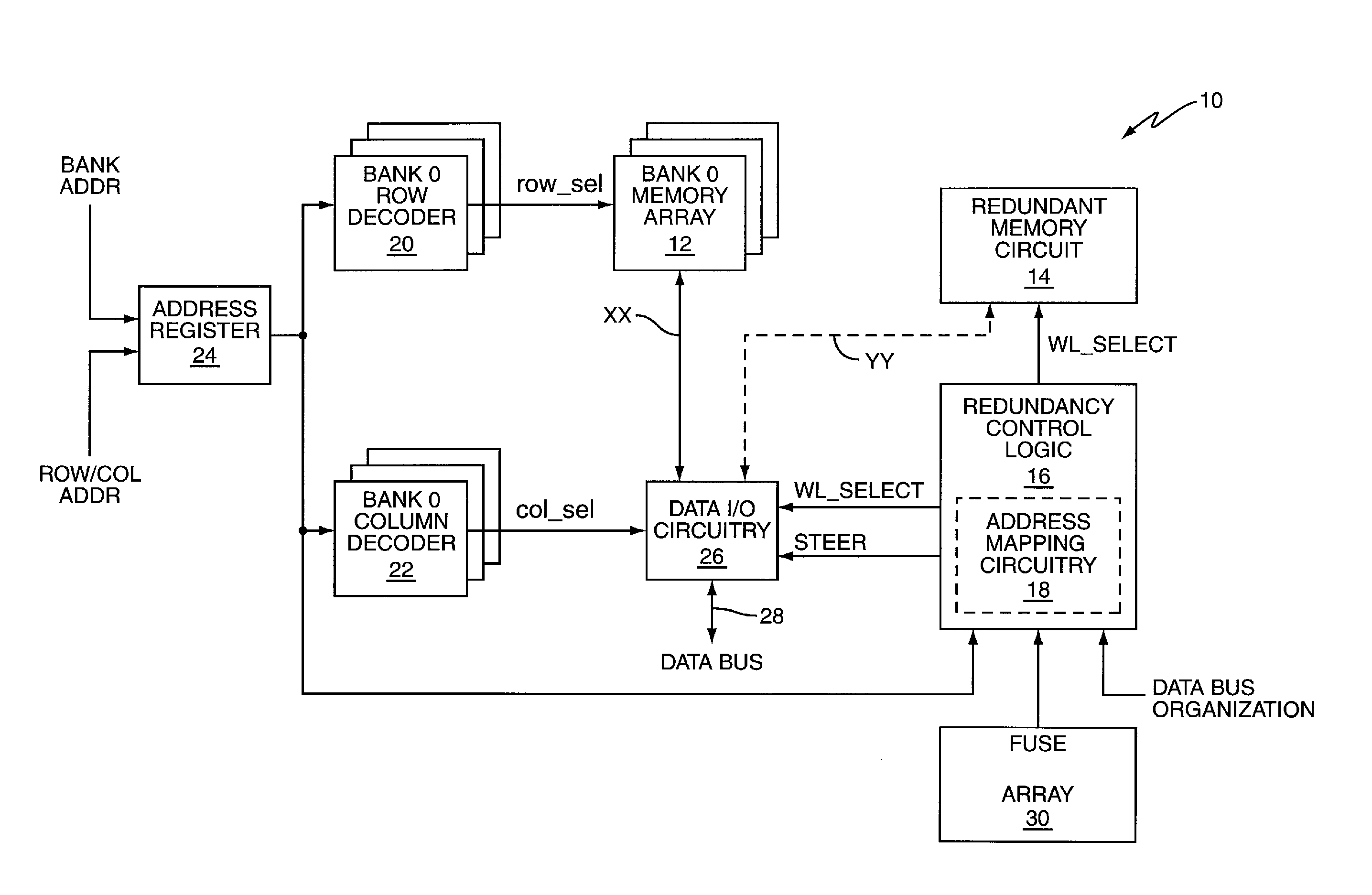
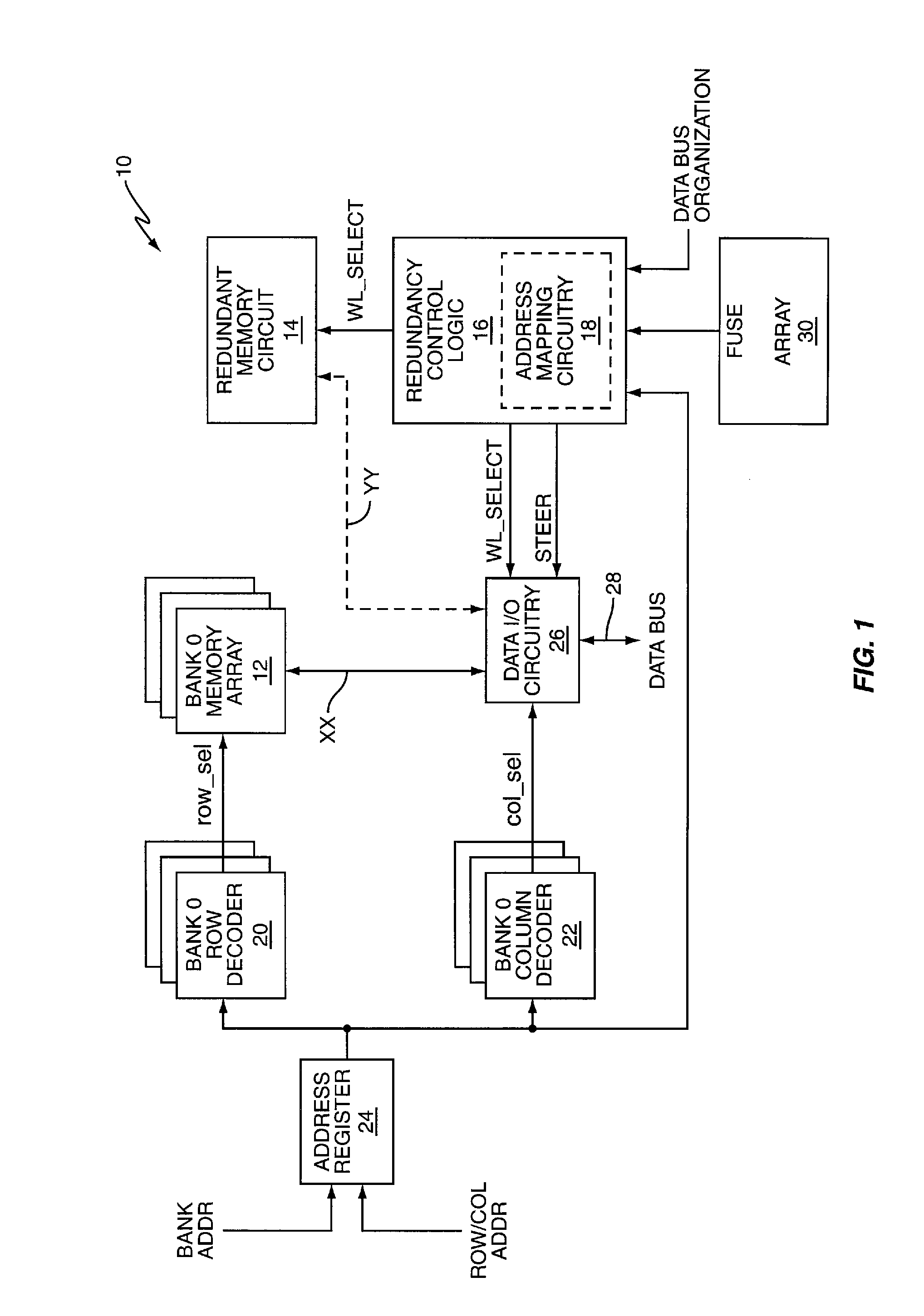
[0013]FIG. 1 illustrates an embodiment of a memory device 10 including a memory array 12 arranged as one or more separately addressable banks of memory cells. The memory array 12 may comprise any kind of volatile or non-volatile memory such as Dynamic Random Access Memory (DRAM), embedded-DRAM, Static Random Access Memory (SRAM), Magneto-resistive Random Access Memory (MRAM), FLASH, etc. The memory device 10 also includes a redundant memory circuit 14 for replacing defective memory locations in the memory array 12. The redundant memory circuit 14 may also comprise any kind of volatile or non-volatile memory such as the kinds previously mentioned.

[0014]Control logic 16 included in the memory device 10 manages access to the redundant memory circuit 14. The redundancy control logic 16 determines when redundancy is implemented and how it is organized. Address mapping circuitry 18 included in or associated with the redundancy control logic 16 segments the redundant memory circuit 14 into...


PUM


Abstract

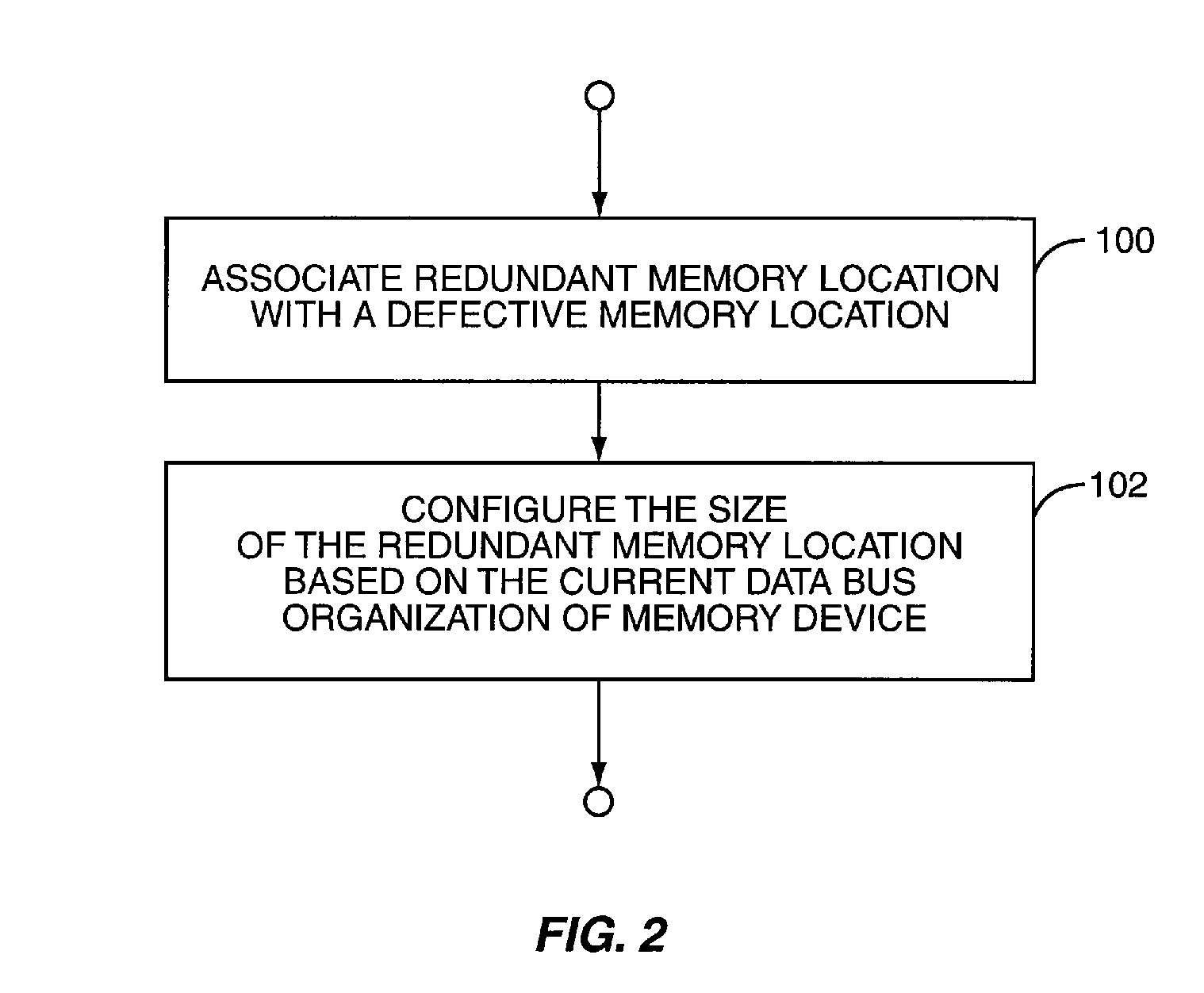
Redundancy is provided in a memory device having a configurable data bus organization by associating a redundant memory location with a defective memory location and configuring a size of the redundant memory location based on the current data bus organization of the memory device.

Description

BACKGROUND OF THE INVENTION[0001]A single failing memory cell amongst millions in a memory device causes failure. Memory devices are tested at several levels of fabrication and assembly to determine whether defective memory cells are present. Identified defects are repaired using redundancy included within a memory device, thus improving manufacturing yields. Redundancy is implemented by replacing a defective memory location with a redundant memory element during normal operation when the defective memory location is addressed.[0002]A fuse array such as a metal or electronic fuse array included in a memory device conventionally stores addresses identifying defective memory locations. The fuse array is programmed during testing responsive to detecting one or more defective memory locations within a memory array. During functional operation, latches capture the state of the fuse array. Latched address information is compared against addresses provided to the memory device during norma...

Claims


Application Information

Patent Timeline
IPC IPC(8): G01R31/28
CPCG11C29/76G11C29/785G11C29/808
Inventor WIENCHOL, HERMANN
Owner QIMONDA
Learn More