Light emitting device and method for making the same

a technology of light-emitting diodes and diodes, which is applied in the manufacture of semiconductor/solid-state devices, semiconductor devices, electrical apparatus, etc., can solve the problems of hardly providing and cannot provide further enhancement in the reduction of threading dislocation density. achieve the effect of low threading dislocation density

Inactive Publication Date: 2008-11-13
EPISTAR CORP
View PDF8 Cites 44 Cited by
  • Summary
  • Abstract
  • Description
  • Claims
  • Application Information

AI Technical Summary

Benefits of technology

[0007]The object of the present invention is to provide a light emitting diode including a roughened epitaxial substrate having roughened ridges that permit an epitaxial layer formed on the epitaxial substrate to exhibit a relatively low threading dislocation density.
[0008]Another object of the present invention is to provide a method for making the light emitting diode that can overcome the aforesaid drawbacks associated with the prior art.

Problems solved by technology

Moreover, for the case of wet etching, the local surfaces of the recessed regions thus formed normally have a relatively low roughness, which can hardly provide further enhancement in the reduction of the threading dislocation density.
However, the local surfaces of the protrusions and the recessed regions thus formed still have a relatively low roughness and remain substantially flat, and thus cannot provide further enhancement in the reduction of the threading dislocation density.

Method used


Image

  • Light emitting device and method for making the same
  • Light emitting device and method for making the same
  • Light emitting device and method for making the same

Examples


example 1

[0034]The light emitting diode of Example 1 was prepared by the following steps.

[0035]A Ni film serving as the mask layer 9 and having a layer thickness of 30 nm was formed on a sapphire substrate 6 using e-beam evaporation techniques at a working temperature of 600° C. The Ni film thus formed was subjected to annealing treatment at an annealing temperature of 600° C. for 10 minutes for permitting atomic migration which led to roughening of the Ni film. The layered structure was then subjected to reactive ion etching (RIE) for removing the Ni film and roughening the sapphire substrate 6. FIG. 6 is an atomic force microscopic (AFM) graph showing a roughened surface of the roughened sapphire substrate 6 with the ridges 61 and valleys 62. The roughness (Ra) of the roughened surface of the sapphire substrate 6 was measured, and was about 10 nm. The roughened sapphire substrate 6 was then placed into a MOCVD system into which a reactant mixture of (CH3)3Ga (TMG):NH3 (gas flow rate ratio=...

example 2

[0036]The light emitting diode of Example 2 was prepared by steps similar to those of Example 1, except that the Ni film formed on the sapphire substrate 6 had a layer thickness of 500 nm, and that the Ni film was removed and the sapphire substrate 6 was roughened using sandblasting techniques under a working pressure of 100 g / cm2 for 5 seconds. SiO2 beads having particle diameters 20 μm, 10 μm, and 5 μm in a ratio of 1:1:1 were used, and the distance between the bead outlet of the nozzle and the Ni film was set at 20 cm. The roughness (Ra) of the roughened surface of the sapphire substrate 6 was measured, and was about 10 nm.

example 3

[0037]The light emitting diode of Example 3 was prepared by steps similar to those of Example 1, except that the Ni film was dispensed with for this Example, and that the sapphire substrate 6 was directly roughened using sandblasting techniques under a working pressure of 2 Kg / cm2 for 60 seconds. SiO2 beads having particle diameters 50 μm, 20 μm, and 10 μm in a ratio of 1:1:1 were used, and the distance between the bead outlet of the nozzle 200 and the Ni film was set at 15 cm. The roughness (Ra) of the roughened surface of the sapphire substrate 6 was measured, and was about 15 nm.

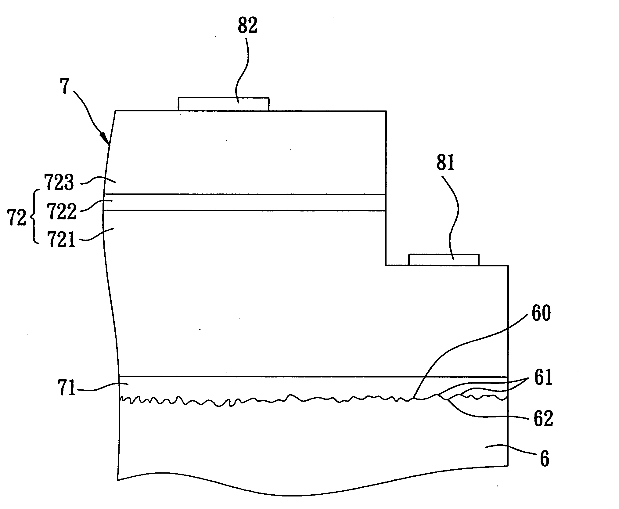
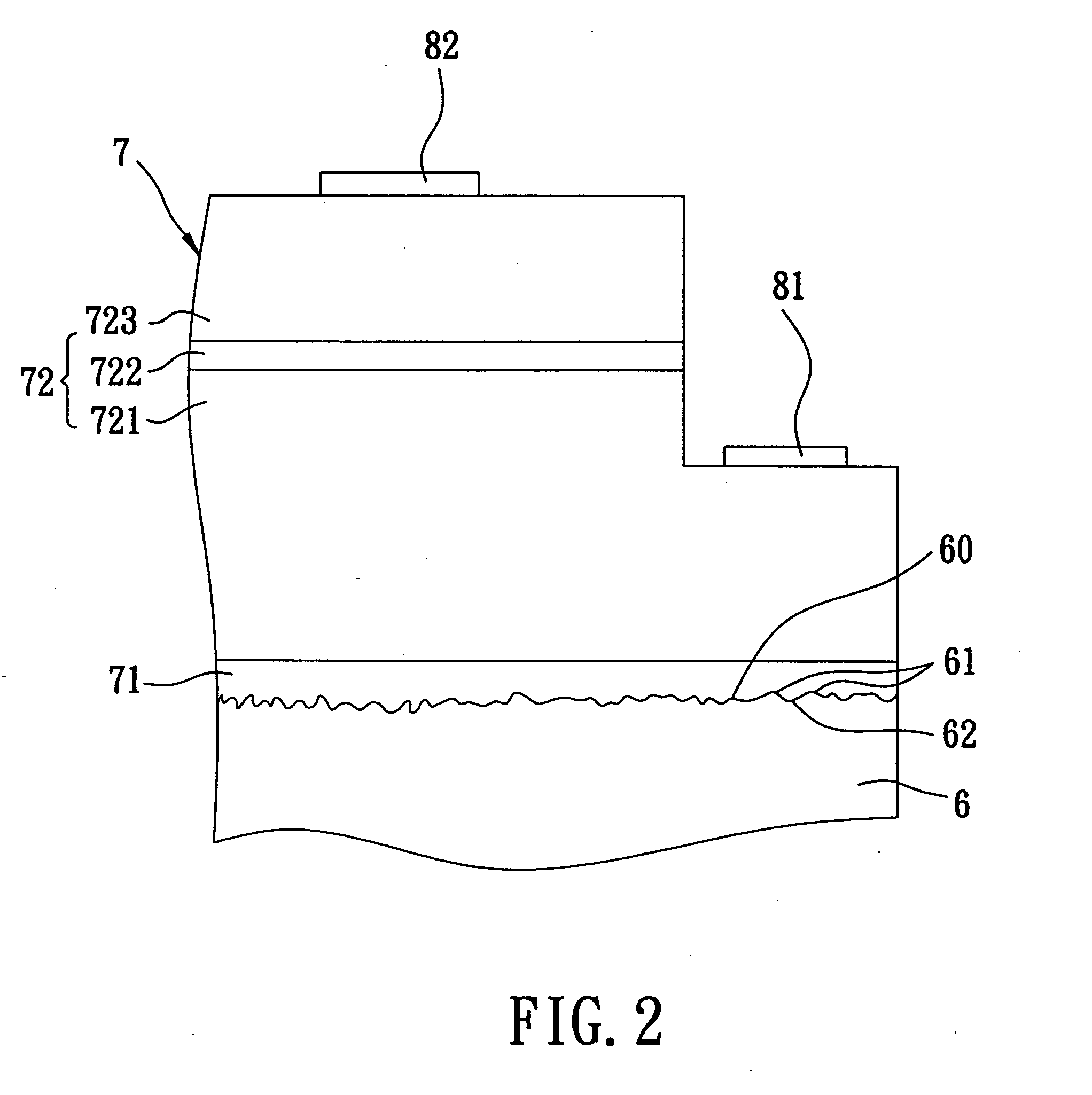
[0038]By forming the epitaxial substrate 6 with the ridges 61 and valleys 62, and by roughening each ridge 61 or each valley 62 with a teeth-like profiled ridgeline according to the method of the present invention, the aforesaid drawbacks associated with the prior art can be eliminated.


PUM


Abstract

A light emitting diode includes: an epitaxial substrate having a roughened side and formed with alternately disposed ridges and valleys at the roughened side, each of the ridges having a roughened surface that is formed with a dense concentration of alternately disposed pits and protrusions; and an epitaxial layered structure formed on and covering the ridges and the valleys of the epitaxial substrate. A method for making the light emitting diode involves forming the epitaxial substrate with the ridges and valleys prior to the formation of the epitaxial layered structure.

Description

BACKGROUND OF THE INVENTION[0001]1. Field of the Invention[0002]This invention relates to a light emitting diode, more particularly to a light emitting diode and a method involving forming an epitaxial layered structure on a roughened epitaxial substrate for making the light emitting diode.[0003]2. Description of the Related Art[0004]It is known in the art that the internal quantum efficiency of a light emitting diode is considerably decreased due to the presence of threading dislocation in an epitaxial crystal layer of the light emitting diode. Threading dislocation is generated when one material is formed on another material, and the larger the lattice mismatch between the two materials, the higher will be the threading dislocation density in said one material.[0005]Referring to FIG. 1, conventional methods for reducing the threading dislocation density in an epitaxial layer 12 of a light emitting diode normally involve formation of recesses 111 in an epitaxial substrate 11, such ...

Claims


Application Information

Patent Timeline
Patent Type & Authority Applications(United States)
IPC IPC(8): H01L33/00H01L33/12H01L33/22
CPCH01L21/0237H01L21/0242H01L21/0254H01L21/02658H01L33/007H01L33/12H01L33/22
Inventor TSAI, TZONG-LIANG
Owner EPISTAR CORP
Why Eureka
Try Eureka