Shift register and shift register apparatus thereof

a shift register and shift register technology, applied in the field of shift register and shift register apparatus thereof, can solve the problems of a-si film deformation, many defects, and often considered less convenient p-type a-si tfts, and achieve the effect of reducing the threshold voltage of a-si tft shift and effective increasing the service life of the shift register apparatus

Inactive Publication Date: 2008-11-13
CHUNGHWA PICTURE TUBES LTD
View PDF11 Cites 24 Cited by
  • Summary
  • Abstract
  • Description
  • Claims
  • Application Information

AI Technical Summary

Benefits of technology

[0011]Accordingly, the present invention is directed to a shift register and a shift register apparatus thereof, wherein degradation of an a-Si thin film due to a gate of an a-Si TFT being applied with a bias voltage for a long time may be avoided, and improvement in the reliability of the a-Si TFT and stability of the circuit may be realized.
[0020]According to another embodiment of the present invention, the shift register apparatus further includes a first buffer circuit. The first buffer circuit is coupled to a common node shared by the pull-up circuit and the pull-down circuit. The common node is adapted for outputting the output signals. The first buffer circuit is adapted for buffering and improving a driving ability of the output signal.
[0027]The present invention employs specific TFT (a-Si TFT) coupling relationship to avoid conventional flip-flop circuit structure. Incorporating with some particular clock pulses to control the on / off states of the a-Si TFTs, the present invention is capable of shifting input signals, while preventing a gate of the a-Si TFT from being applied with a bias for a long time. According to the present invention, not only the a-Si thin film of the a-Si TFT is not likely to be degraded improve the reliability of the a-Si TFT, but also the shift of the threshold voltage of the a-Si TFT can be minimized, so as to allow the output voltage to be completely charged. Therefore, the service life of the shift register apparatus can be effectively increased.

Problems solved by technology

Therefore, P-type a-Si TFTs are often considered as less convenient than N-type a-Si TFTs.
However, such a bias configuration negatively affects the inverter circuit, in that if the gate of the a-Si TFT is applied with a direct current bias for a relative long time, the a-Si film will be degraded and incur many defects.
In the meantime, a threshold voltage Vt thereof inevitably is significant.
Therefore, the inverter circuit is not suitable for long time operation.
However, the problem of the shift of the threshold voltage of the a-Si TFT occurred after long time use has not yet been resolved. FIG. 2 is a circuit of a shift register apparatus disclosed in U.S. Pat. No. 7,038,653.
This problem drastically shortens a lifetime of the shift register apparatus.
However, when the shift register apparatus is operated, residual charges on a node P2 cannot be discharged therefrom, and a transistor 301 also suffers a bias voltage for a relative long time.
After the shift register apparatus is being operated for an excessively long time, a threshold voltage of the transistor 301 increases drastically, so that a voltage at an output terminal OUTPUT can not be completely charged, and thus the shift register apparatus may be out of use for quite a long time.
However, no effective solution has been found so far.

Method used


Image

  • Shift register and shift register apparatus thereof
  • Shift register and shift register apparatus thereof
  • Shift register and shift register apparatus thereof

Examples


Embodiment Construction

[0040]Reference will now be made in detail to the present preferred embodiments of the invention, examples thereof are illustrated in the accompanying drawings. Wherever possible, the same reference numbers are used in the drawings and the description to refer to the same or like parts.

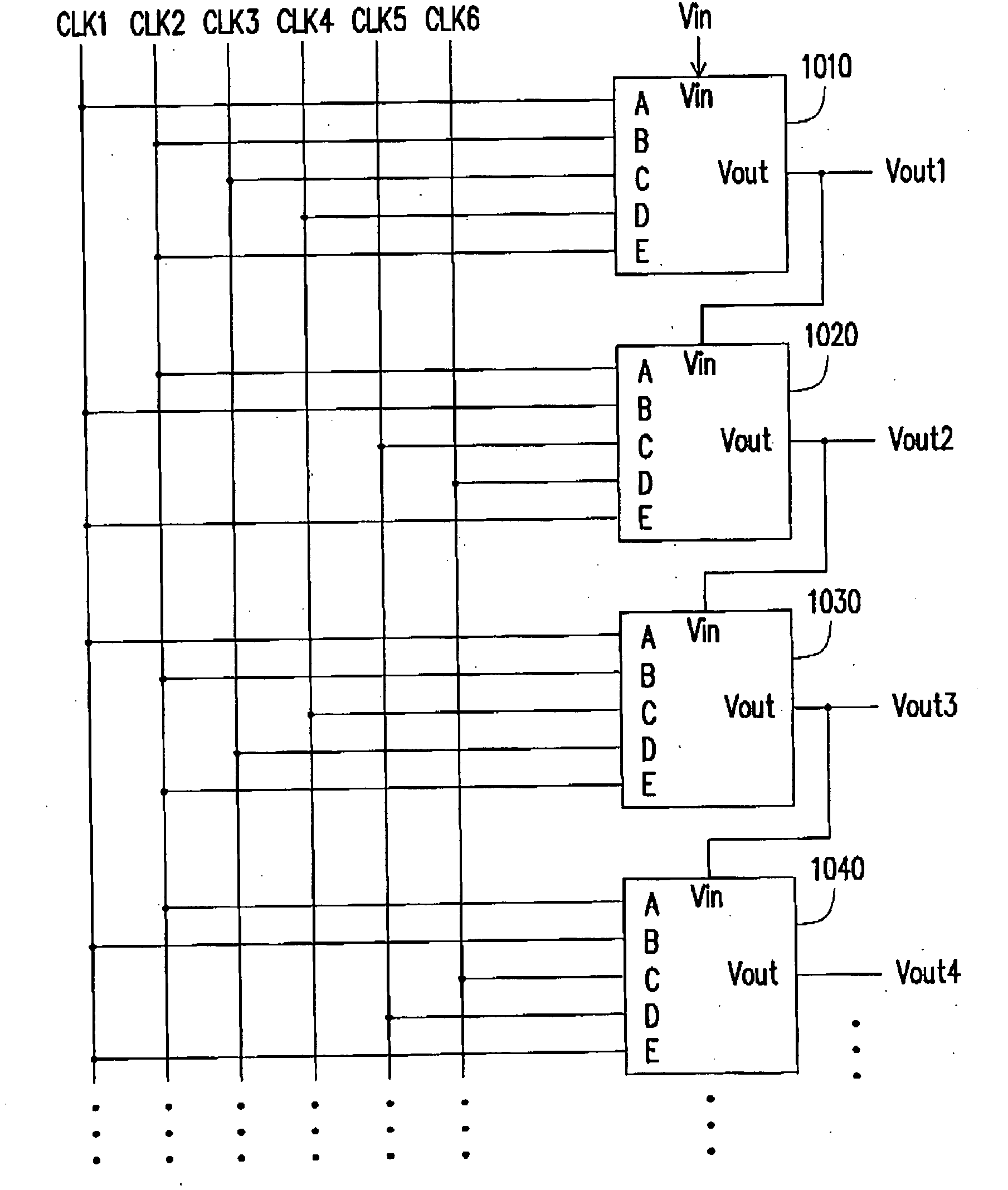
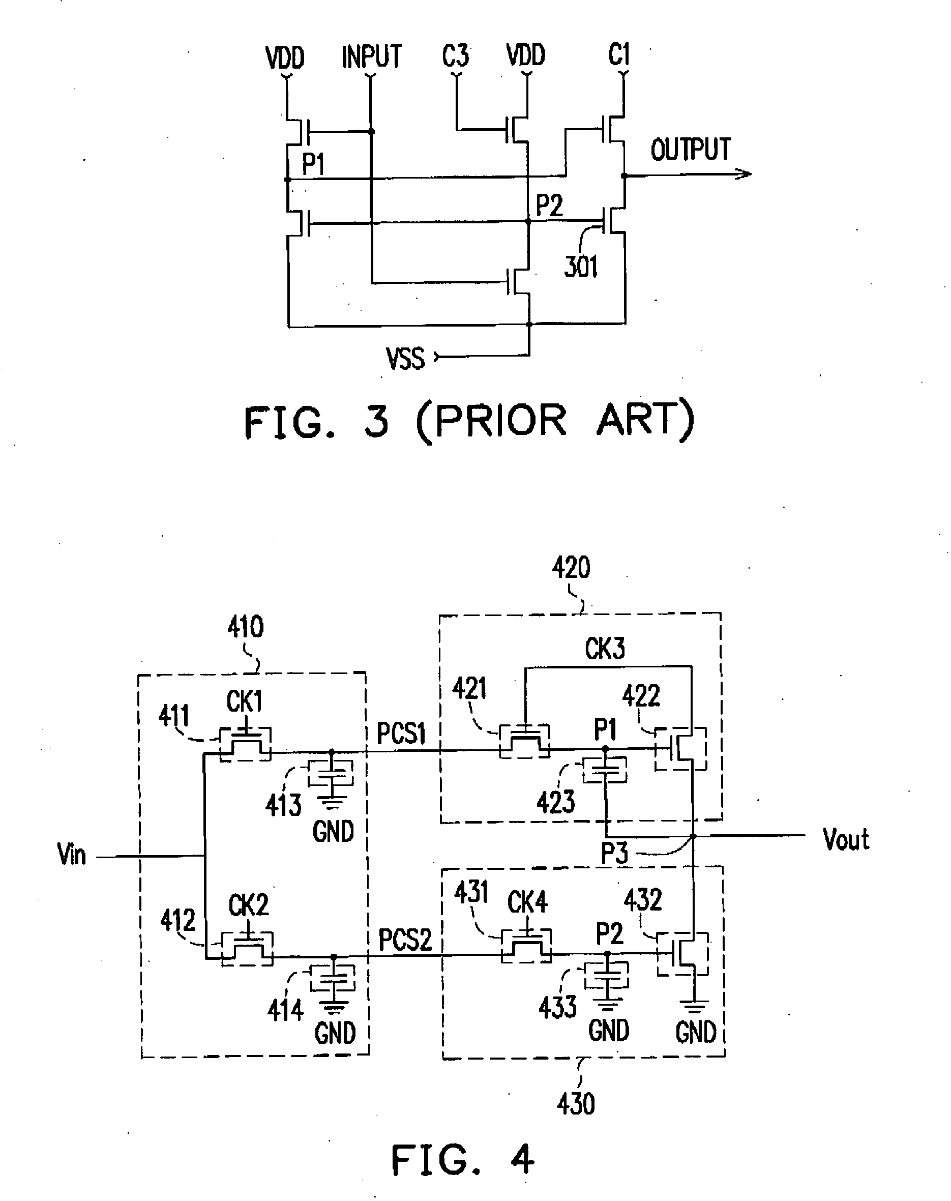
[0041]FIG. 4 is a circuit diagram of a shift register apparatus according to an embodiment of the present invention. Referring to FIG. 4, the shift register apparatus includes a pre-charge circuit 410, a pull-up circuit 420 and a pull-down circuit 430. The pre-charge circuit 410 is adapted to sample input signal Vin according to clock signals CK1 and CK2 for generating charging signal PCS1 and PCS2, respectively. The pull-up circuit 420 is coupled to the pre-charge circuit 410 for receiving a clock signal CK3 and the charging signal PCS1, so as to output an output signal Vout. The pull-down circuit 430 is coupled to the pre-charge circuit 410 and the pull-up circuit 420 for receiving clock signal CK4 ...


PUM


Abstract

A shift register and a shift register apparatus are provided. The shift register includes a plurality of shift register apparatus, and each shift register apparatus comprises a pre-charge circuit, a pull-up circuit and a pull-down circuit. The pre-charge circuit is used for sampling an input signal according to a first clock signal and a second clock signal respectively and generate a first charging signal and a second charging signal respectively. The pull-up circuit is coupled to the pre-charge circuit. The pull-up circuit receives the third clock signal and the first charging signal to output an output signal accordingly. The pull-down circuit is coupled to the pre-charge circuit and the pull-up circuit. The pull-down circuit receives the fourth clock signal and the second charging signal to decide whether to couple the output signal to a common potential.

Description

CROSS-REFERENCE TO RELATED APPLICATION[0001]This application claims the priority benefit of Taiwan application serial no. 96116475, filed on May 9, 2007. The entirety of the above-mentioned patent application is hereby incorporated by reference herein and made a part of this specification.BACKGROUND OF THE INVENTION[0002]1. Field of the Invention[0003]The present invention generally relates to a shift register and a shift register apparatus thereof, and more particularly, to a shift register for avoiding an output voltage incapable of being completely charged due to a bias applied to a gate of an amorphous silicon thin film transistor (a-Si TFT) for a long time and a shift register apparatus thereof[0004]2. Description of Related Art[0005]In a condition of a predetermined panel processing, it is critical for configuring a circuit on a glass substrate to be used an a-Si TFT. Generally, a-Si TFTs can be divided into two types, P-type a-Si TFTs and N-type a-Si TFTs. The P-type a-Si TFT...

Claims


Application Information

Patent Timeline
Patent Type & Authority Applications(United States)
IPC IPC(8): G11C19/00
CPCG11C19/184G11C27/024
Inventor LIU, CHIN-WEITAI, YA-HSIANG
Owner CHUNGHWA PICTURE TUBES LTD
Why Eureka
Try Eureka