

Gallium nitride-on-silicon interface
- Summary
- Abstract
- Description
- Claims
- Application Information
AI Technical Summary
Benefits of technology
Problems solved by technology
Method used
Image

Examples
Embodiment Construction
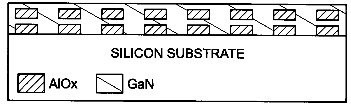
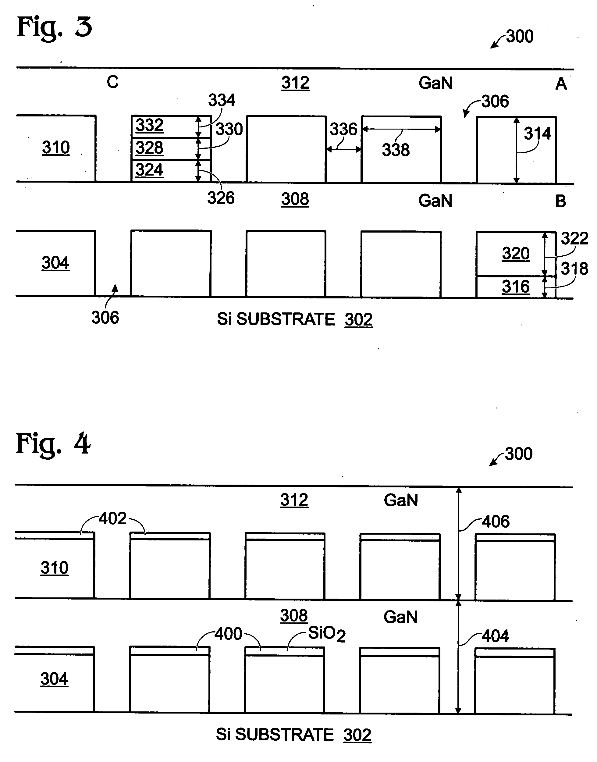
[0026]FIG. 3 is a partial cross-sectional view of a silicon (Si)-to-gallium nitride (GaN) thermal expansion interface. The interface 300 comprises a Si substrate 302 with a crystallographic orientation of (111). A first aluminum (Al)-containing film 304 in compression overlies the Si substrate 302, with nano-column holes 306 in the Al-containing film 304 exposing regions of the underlying Si substrate 302. A first layer of GaN 308 is formed in the nano-column holes 306 and overlying the first Al-containing film 304. A second Al-containing film 310 in compression overlies the first GaN layer 308, with nano-column holes 306 in the second Al-containing film 310, exposing regions of the underlying first GaN layer 308. A second GaN layer 312 is formed in the nano-column holes 306 and overlying the second Al-containing film 310.
[0027]In one aspect (detail A), the first and second Al-containing films 304 and 310 are an AlN film having a thickness 314 in a range of about 5 to 500 nanometers...
PUM
 Abstract
Description
Claims
Application Information