Supercharge Your Innovation With Domain-Expert AI Agents!

Chip Package with Stiffener Ring

a technology of stiffener ring and chip package, which is applied in the direction of semiconductor devices, semiconductor/solid-state device details, electrical apparatus, etc., can solve the problems of reducing electrical pathways without inducing potentially damaging substrate warping, and the tendency of conventional substrates to still warp

Inactive Publication Date: 2008-11-20
GLOBALFOUNDRIES INC
View PDF28 Cites 33 Cited by
  • Summary
  • Abstract
  • Description
  • Claims
  • Application Information

AI Technical Summary

Problems solved by technology

Even with that provided stiffness, conventional substrates still tend to warp due to mismatches in coefficients of thermal expansion for the chip, underfill and substrate.
The difficult problem is how to reduce the electrical pathways without inducing potentially damaging substrate warping.

Method used


Image

  • Chip Package with Stiffener Ring
  • Chip Package with Stiffener Ring
  • Chip Package with Stiffener Ring

Examples


Embodiment Construction

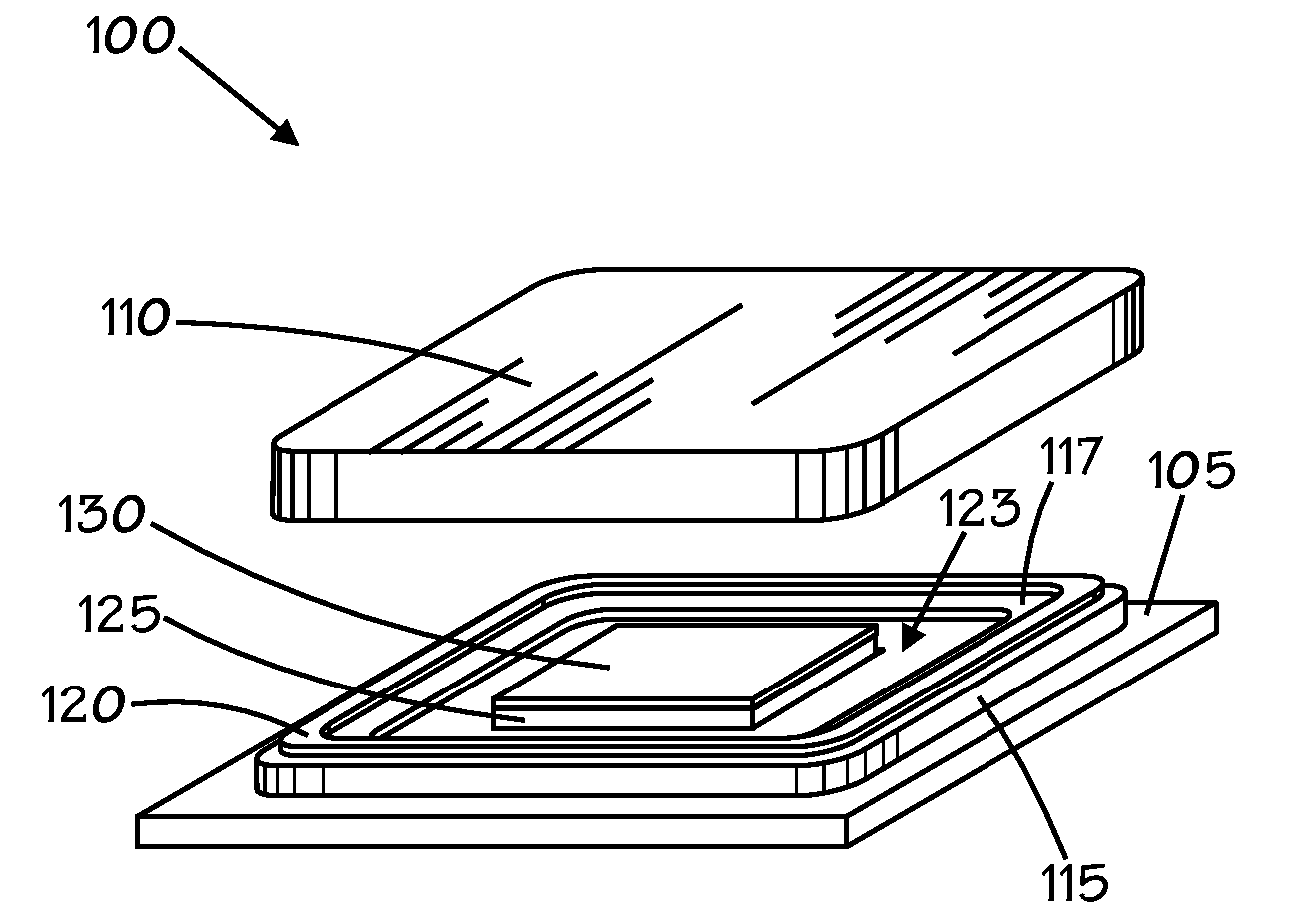
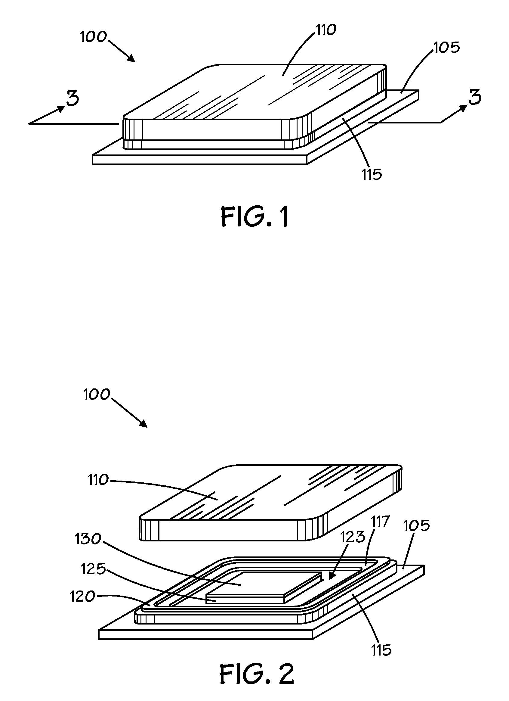
[0025]In the drawings described below, reference numerals are generally repeated where identical elements appear in more than one figure. Turning now to the drawings, and in particular to FIG. 1, therein is shown a pictorial view of an exemplary embodiment of an integrated circuit package 100 that includes a substrate 105, an overlying lid 110 and a stiffener ring 115. The stiffener ring 115 is sandwiched between the substrate 105 and the lid 110. The substrate 105 is advantageously a land grid array (“LGA”) but may optionally be a pin grid array, a ball grid array or other type of mountable substrate as desired. The lid 110 covers an integrated circuit (not visible) that is mounted on the substrate 105. Optionally, the package 100 may be lidless, partially or completely overmolded, or glob topped.

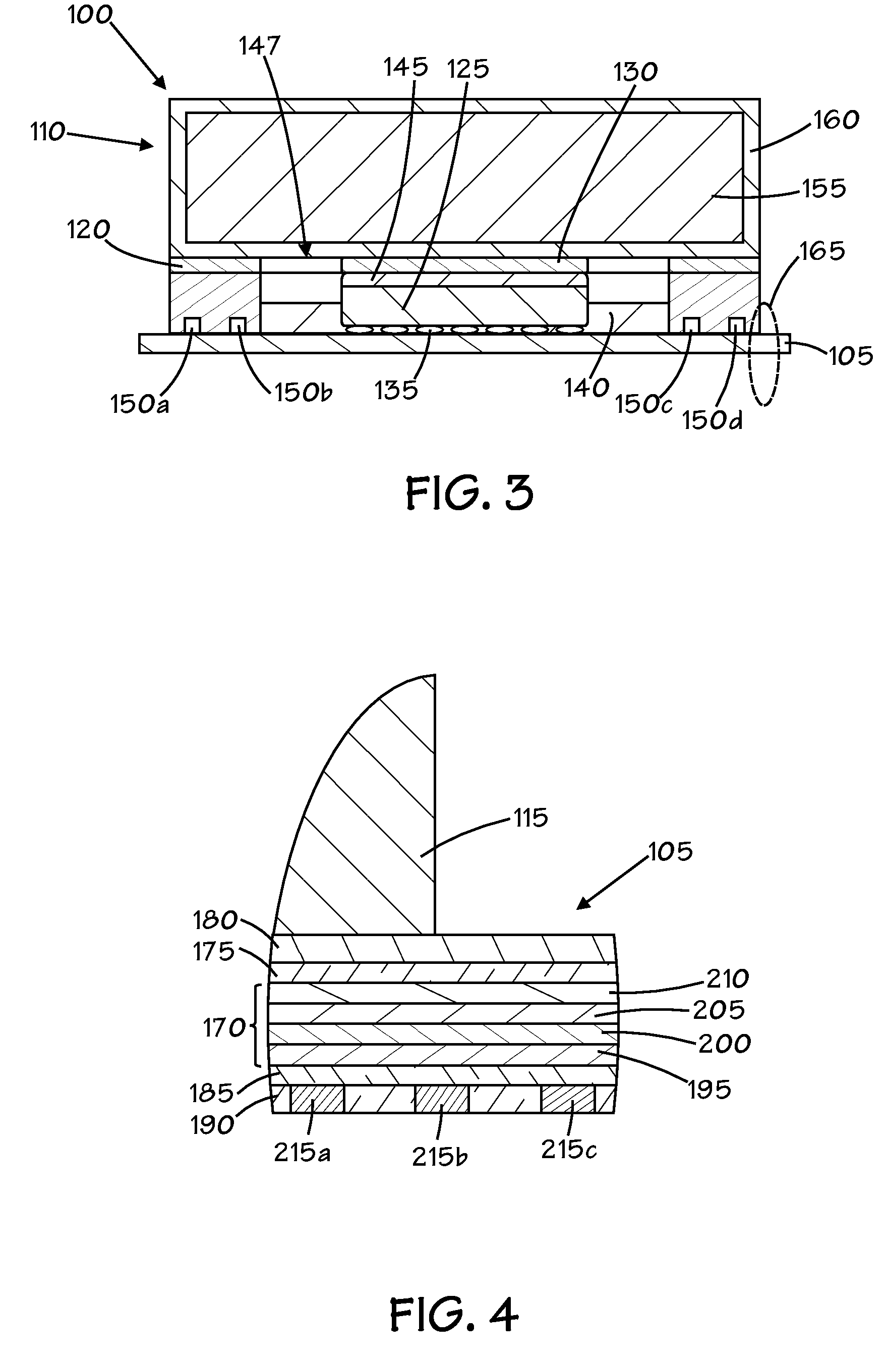
[0026]Additional detail regarding the structure of the package 100 may be understood by referring now also to FIG. 2, which is a pictorial view like FIG. 1 but with the lid 110 exploded fr...


PUM


Abstract

Various semiconductor chip packages and methods of making the same are provided. In one aspect, a method of manufacturing is provided that includes providing a substrate that has a first side and a first plurality of passive devices in the first side. A polymeric stiffener ring is formed on the first side. The stiffener ring embeds the first plurality of passive devices without covering a central portion of the first surface of the substrate. A semiconductor chip is mounted on the central portion of the first surface of the substrate.

Description

BACKGROUND OF THE INVENTION[0001]1. Field of the Invention[0002]This invention relates generally to semiconductor processing, and more particularly to semiconductor chip packaging and to methods of making the same.[0003]2. Description of the Related Art[0004]Many current integrated circuits are formed as multiple die on a common silicon wafer. After the basic process steps to form the circuits on the die are complete, the individual die are cut from the wafer. The cut die are then usually mounted to structures, such as circuit boards, or packaged in some form of enclosure.[0005]One frequently-used package consists of a substrate upon which a die is mounted. The upper surface of the substrate includes electrical interconnects. The die is manufactured with a plurality of bond pads. A collection of solder bumps are provided between the bond pads of the die and substrate interconnects to establish ohmic contact. An underfill material is deposited between the die and the substrate to act...

Claims


Application Information

Patent Timeline
IPC IPC(8): H01L23/28H01L21/00
CPCH01L23/053H01L23/10H01L23/16H01L2224/73253H01L2224/16225H01L2924/00011H01L2924/00014H01L2924/15312H01L2924/19105H01L2224/0401
Inventor TOSAYA, ERICZHAI, JUNLEONG, CHIA-KENLEY, TOM
Owner GLOBALFOUNDRIES INC
Features
  • R&D
  • Intellectual Property
  • Life Sciences
  • Materials
  • Tech Scout
  • Unparalleled Data Quality
  • Higher Quality Content
  • 60% Fewer Hallucinations
Learn More