

Method for manufacturing semiconductor package
- Summary
- Abstract
- Description
- Claims
- Application Information
AI Technical Summary
Benefits of technology
Problems solved by technology
Method used
Image

Examples
Embodiment Construction
[0026]Exemplary embodiments of the present invention will now be described in detail with reference to the accompanying drawings.
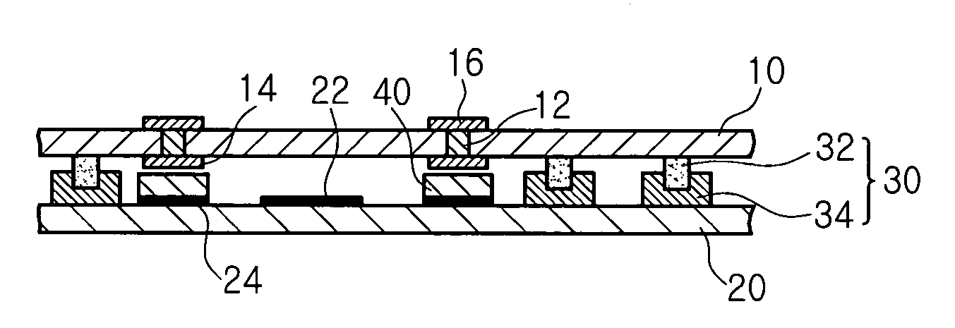
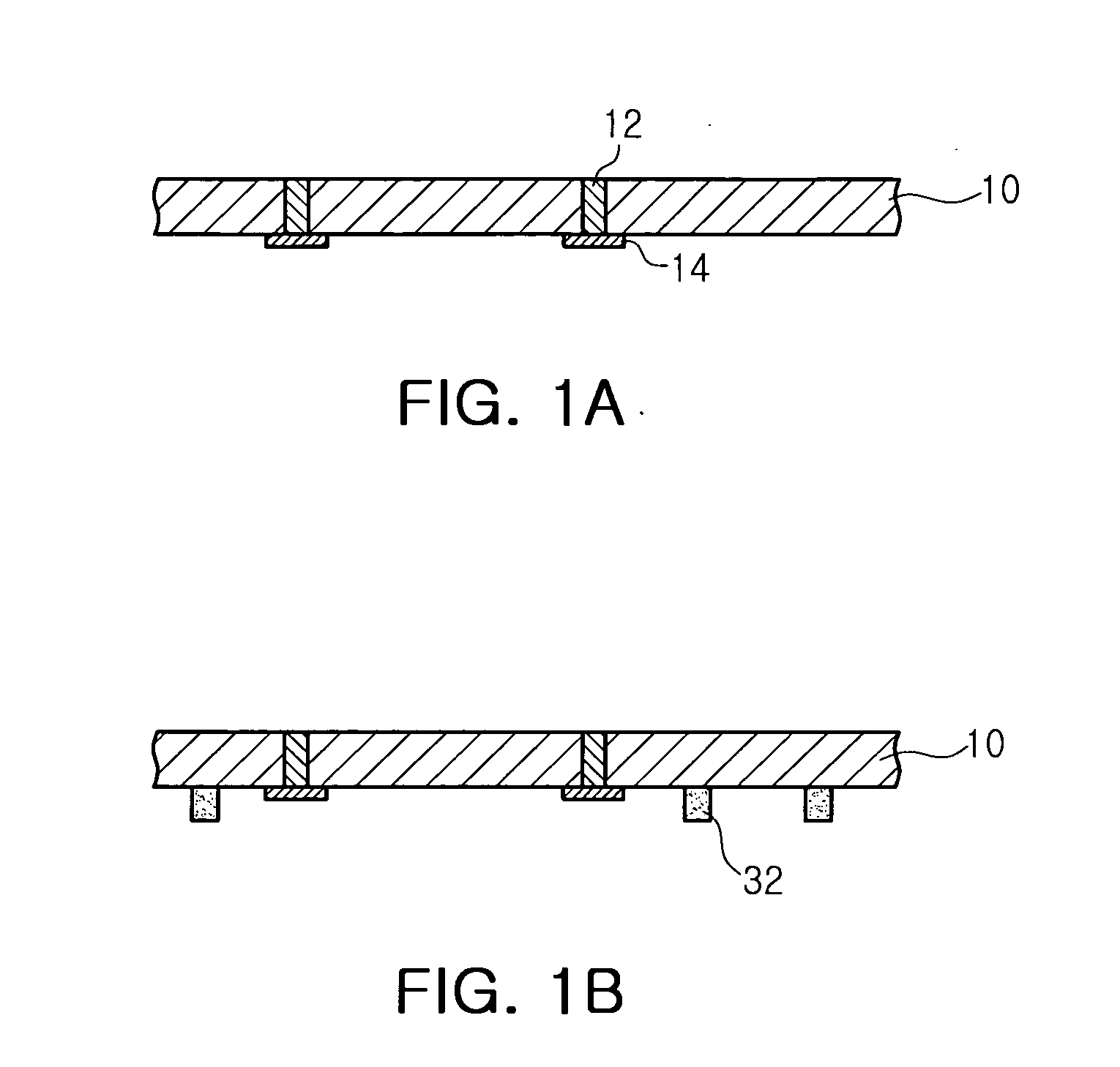
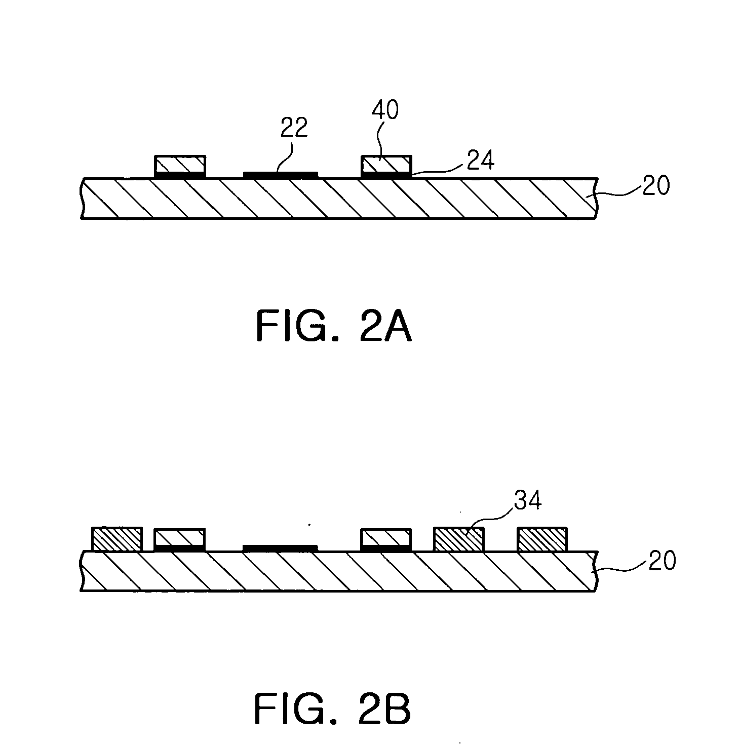
[0027]FIGS. 1A and 1B are cross-sectional views illustrating providing a wafer for a cap substrate according to the present invention, FIGS. 2A and 2B are cross-sectional views illustrating providing a wafer for a device substrate according to the present invention, FIGS. 3A and 3B are cross-sectional views illustrating primarily bonding a wafer for a cap substrate and a wafer for a device substrate according to the present invention, FIGS. 4A, 4B, and 4C are cross-sectional views illustrating secondarily bonding a wafer for a cap substrate and a wafer for a device substrate according to the present invention, and FIG. 5 is a cross-sectional view illustrating a wafer for a cap substrate and a wafer for a device substrate according to another embodiment of the present invention.
[0028]Referring to FIG. 1A, in an operation of providing the wafer 10 for the ca...
PUM
 Abstract
Description
Claims
Application Information