Field emission display having an improved emitter structure

a field emission display and emitter technology, applied in the field of field emission displays, can solve the problems of high manufacturing cost, clear limit in manufacturing a wide screen fed, and high equipment cost, and achieve the effects of improving the focusing characteristics of electron beams, improving image quality, and controlling the amount of dispersion of electron beams

Inactive Publication Date: 2008-11-27
OH TAE SIK
View PDF8 Cites 0 Cited by
  • Summary
  • Abstract
  • Description
  • Claims
  • Application Information

AI Technical Summary

Benefits of technology

[0011]It is also an object of the present invention to provide a design for an FED that improves image quality by better controlling the amount of dispersion of electron beams emanating from an emitter.
[0012]It is also an object of the present invention to provide an FED and an emitter design that improves the focusing characteristics of electron beams emanating from the emitter.
[0013]It is still an object of the present invention to provide an improved design for an emitter in an FED that results in an improved image quality.

Problems solved by technology

In order to arrange such metallic tip-type emitter in an FED, however, an ultramicroscopic hole should be formed, and molybdenum should be evenly deposited on the entire surface of a screen, which requires the use of difficult techniques and expensive equipment and thus results in an increase in manufacturing costs.
Therefore, there is a clear limit in manufacturing a wide screen FED.

Method used


Image

  • Field emission display having an improved emitter structure
  • Field emission display having an improved emitter structure
  • Field emission display having an improved emitter structure

Examples


Embodiment Construction

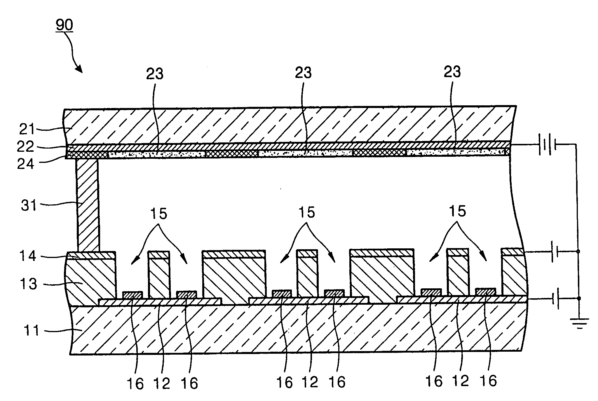
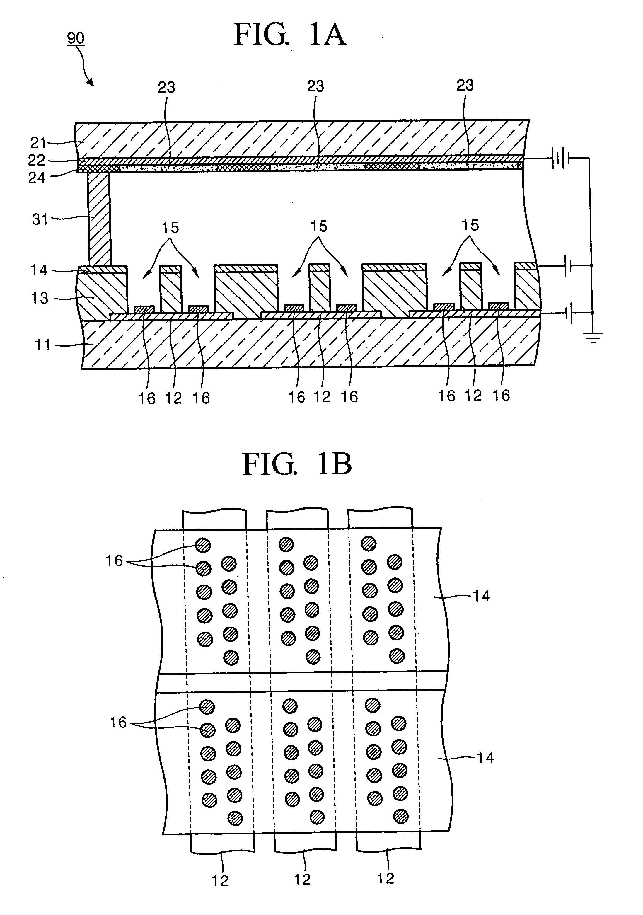
[0036]Turning now to the figures, FIGS. 1A and 1B are a cross-sectional view and a plan view, respectively, of an FED 90. Referring to FIGS. 1A and 1B, the FED 90 has a triode structure made of a cathode electrode 12, an anode electrode 22, and a gate electrode 14. The cathode electrode 12 and the gate electrode 14 are formed on a rear substrate 11, and the anode electrode 22 is formed at the bottom of a front substrate 21. A fluorescent layer 23 is formed of R, G, and B fluorescent materials, and a black matrix 24 is formed on the bottom surface of the anode electrode 22 so as to improve contrast. The rear substrate 11 and the front substrate 21 are a predetermined distance apart from each other. The predetermined distance between the rear substrate 11 and the front substrate 21 is maintained by a spacer 31 disposed between the rear substrate 11 and the front substrate 21. When manufacturing the FED 90, the cathode electrode 12 is formed on the rear substrate 11, an insulation laye...


PUM


Abstract

A field emission display (FED) is provided. The FED has an emitter structure where the emitter, a conductor and a cathode electrode are so arranged to produce a certain electric field about the emitter. The electric field about the emitter causes the electron beam emitted from the emitter to have improved focus and have less dispersion. This causes the electron beam to hit the intended pixel without exciting phosphor layers in neighboring pixels, thus improving image quality.

Description

BACKGROUND OF THE INVENTION[0001]This application claims the priority of Korean Patent Application Nos. 2003-84963 and 2004-35534, filed on Nov. 27, 2003 and May 19, 2004, respectively, in the Korean Intellectual Property Office, the disclosures of which are incorporated herein in their entirety by reference.[0002]1. Field of the Invention[0003]The present invention relates to a field emission display and, more particularly, to a field emission display having an emitter structure that improves focusing characteristics of electron beams, thus improving image quality.[0004]2. Description of the Related Art[0005]Display devices, which account for one of the most important parts of conventional data transmitting media, have been used in personal computers and television receivers. The display devices include cathode ray tubes (CRTs), which use high-speed heat electron emission, and flat panel displays, such as a liquid crystal display (LCD), a plasma display panel (PDP), and a field emi...

Claims


Application Information

Patent Timeline
Patent Type & Authority Applications(United States)
IPC IPC(8): H01J1/62H01J1/30H01J31/12
CPCH01J31/12H01J31/123H01J31/127B01D24/38B01D24/4642F16K5/0605F16K27/067
Inventor OH, TAE-SIK
Owner OH TAE SIK
Why Eureka
Try Eureka