

Switching regulator having reverse current detector
a switching regulator and detector technology, applied in the direction of electric variable regulation, process and machine control, instruments, etc., can solve the problems of reducing power waste, and inability of comparator to carry out comparison operations with high accuracy, so as to improve the efficiency of power conversion under light load conditions
- Summary
- Abstract
- Description
- Claims
- Application Information
AI Technical Summary
Benefits of technology
Problems solved by technology
Method used
Image

Examples
example 1
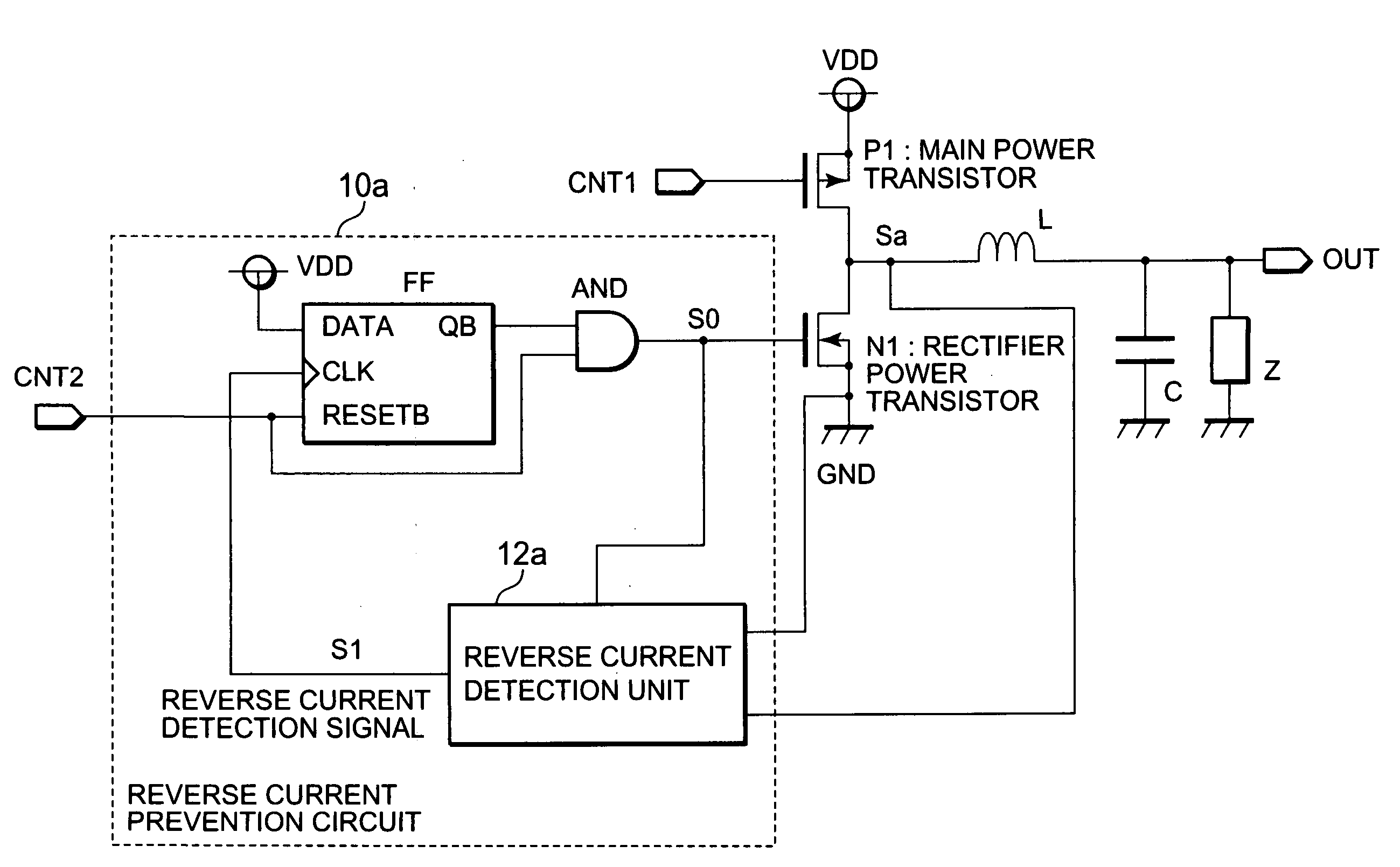
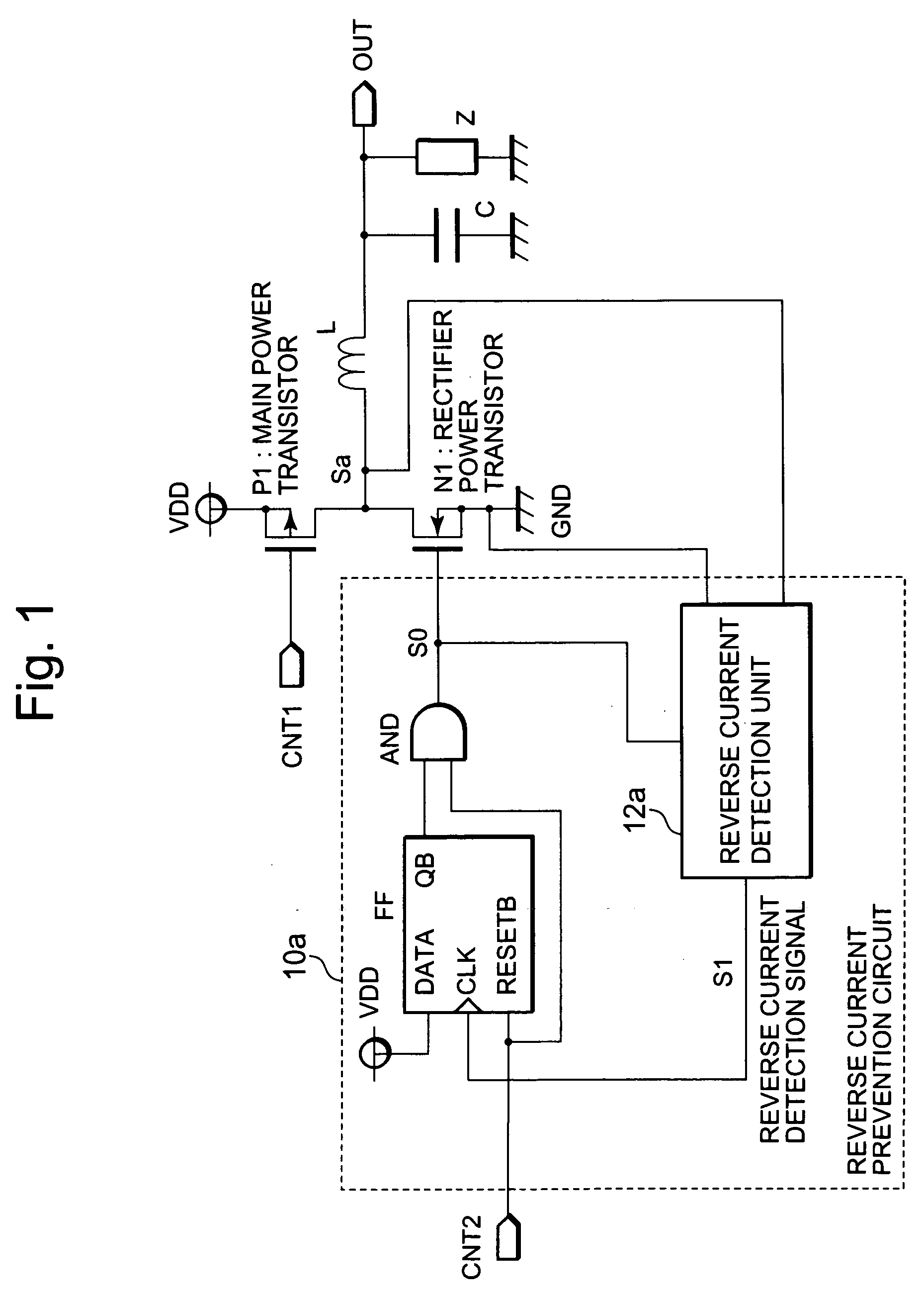
[0030]FIG. 1 is a block diagram showing a configuration of a switching regulator according to a first example of the present invention. In FIG. 1, the switching regulator includes a switching transistor (main power transistor) P1, a synchronous rectifier transistor (rectifier power transistor) N1, a reverse current prevention circuit 10a, an inductor L, and a capacitor C. The switching regulator steps down the voltage from a power source VDD to apply resultant voltage to a load Z.
[0031]The switching transistor P1 is connected to the power source VDD at its source, and is connected to one end of the inductor L at its drain. Moreover, the gate of the switching transistor P1 is provided with a pulse-width or pulse-density modulated control signal CNT1 for controlling output voltage to the load Z.
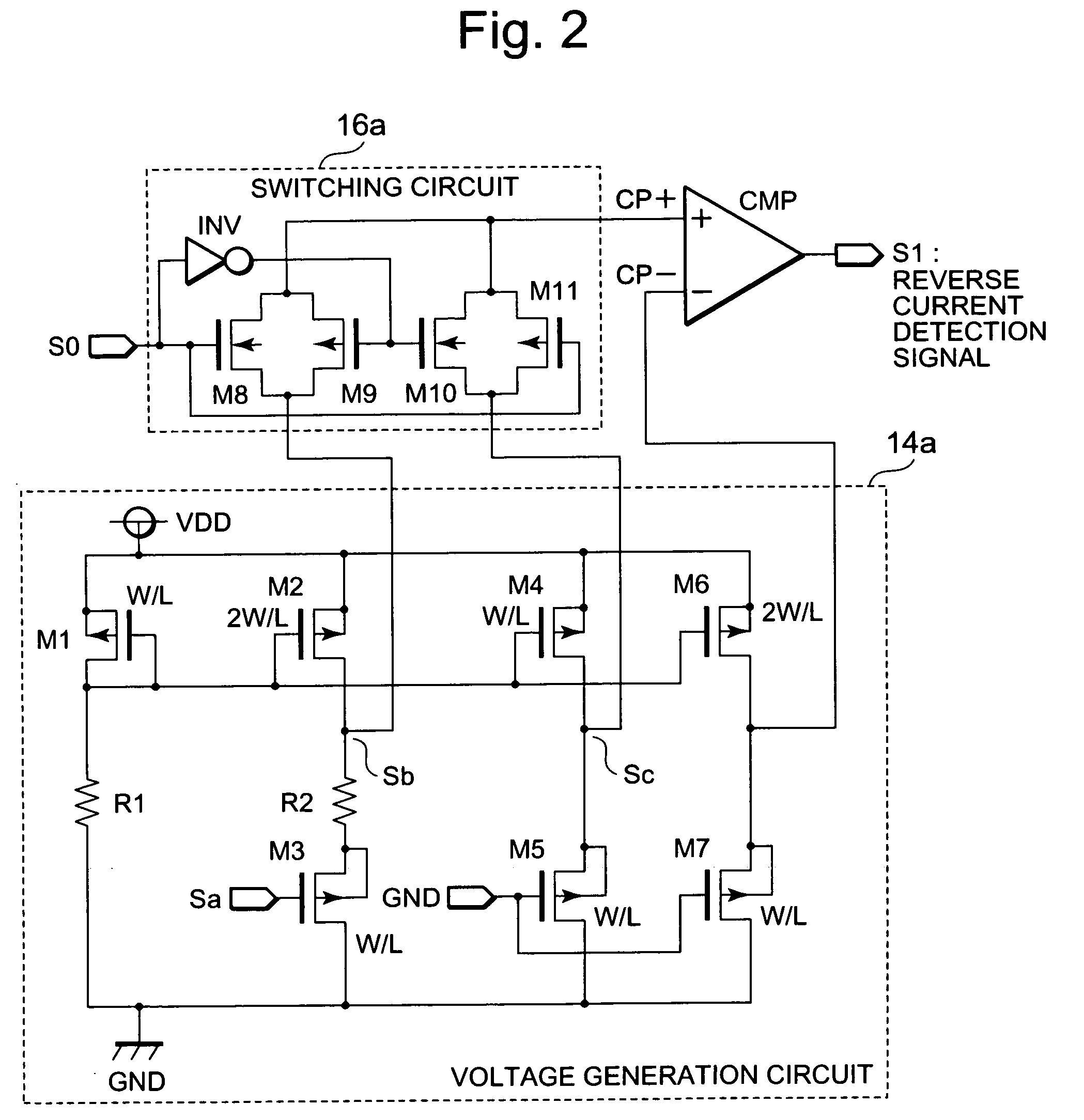
[0032]The synchronous rectifier transistor N1 is connected to ground at its source, and is connected to the one end of the inductor L at its drain. Moreover, the reverse current prevention circ...
example 2
[0067]FIG. 5 is a block diagram showing a configuration of a switching regulator according to a second example of the present invention. In FIG. 5, the same symbols as those used in FIG. 1 are used for denoting the same constituents. The switching regulator in FIG. 5 includes a switching transistor (main power transistor) N2, a synchronous rectifier transistor (rectifier power transistor) P2, a reverse current prevention circuit 10b, a diode D, the inductor L, and the capacitor C. The switching regulator steps up the voltage from the power source VDD to apply the resultant voltage to the load Z connected to the output terminal OUT.
[0068]The switching transistor N2 is connected to ground at its source, and to one end of the inductor L at its drain, and the gate of the switching transistor N2 is provided with a pulse-width or pulse-density modulated control signal CNT1a for controlling output voltage to the load Z.
[0069]The synchronous rectifier transistor P2 is connected, at its sour...
PUM
 Abstract
Description
Claims
Application Information