Display device, driving method thereof, and electronic device

a display device and driving method technology, applied in the direction of electric digital data processing, instruments, computing, etc., can solve the problems of difficulty in realizing a large and high definition display, and achieve the effect of providing a margin for the layout area of the screen, large output buffer, and relatively small layout area

Active Publication Date: 2008-11-27
JOLED INC
View PDF4 Cites 27 Cited by
  • Summary
  • Abstract
  • Description
  • Claims
  • Application Information

AI Technical Summary

Benefits of technology

[0017]Each pixel in the display device according to the above-described embodiment of the present invention includes a drive transistor, a sampling transistor, a retaining capacitance, and a light emitting element. In the above-described embodiment of the present invention, a switching transistor is added to the pixel, and a P-channel type transistor is used as the drive transistor. By thus forming the pixel circuit with the three transistors and using a P-channel type transistor as the drive transistor, it is possible to fix the power supply voltage supplied to each pixel. The power fixation eliminates the need for a power supply scanner, and it can provide a margin for the layout area of the screen. Although another scanner is necessary to perform the line-sequential driving of the switching transistor added to each pixel, this scanner does not need to supply a power supply pulse. Therefore, a large output buffer is not demanded, and the layout area is relatively small. Unlike a power supply scanner, an ordinary scanner for supplying a gate pulse for controlling the switching transistor is degraded to a small degree, and is thus highly reliable. By thus doing away with the power supply scanner that has been demanded in the past, it is possible to increase the layout area of the pixel array unit and improve the reliability of the peripheral driving unit. At the same time, by using a P-channel type transistor as the drive transistor, it is possible to reduce an error in the mobility correcting operation, and thus obtaining high uniformity.

Problems solved by technology

The former system offers a simple structure, but presents, for example, the problem of difficulty in realizing a large and high definition display.

Method used


Image

  • Display device, driving method thereof, and electronic device
  • Display device, driving method thereof, and electronic device
  • Display device, driving method thereof, and electronic device

Examples


first embodiment

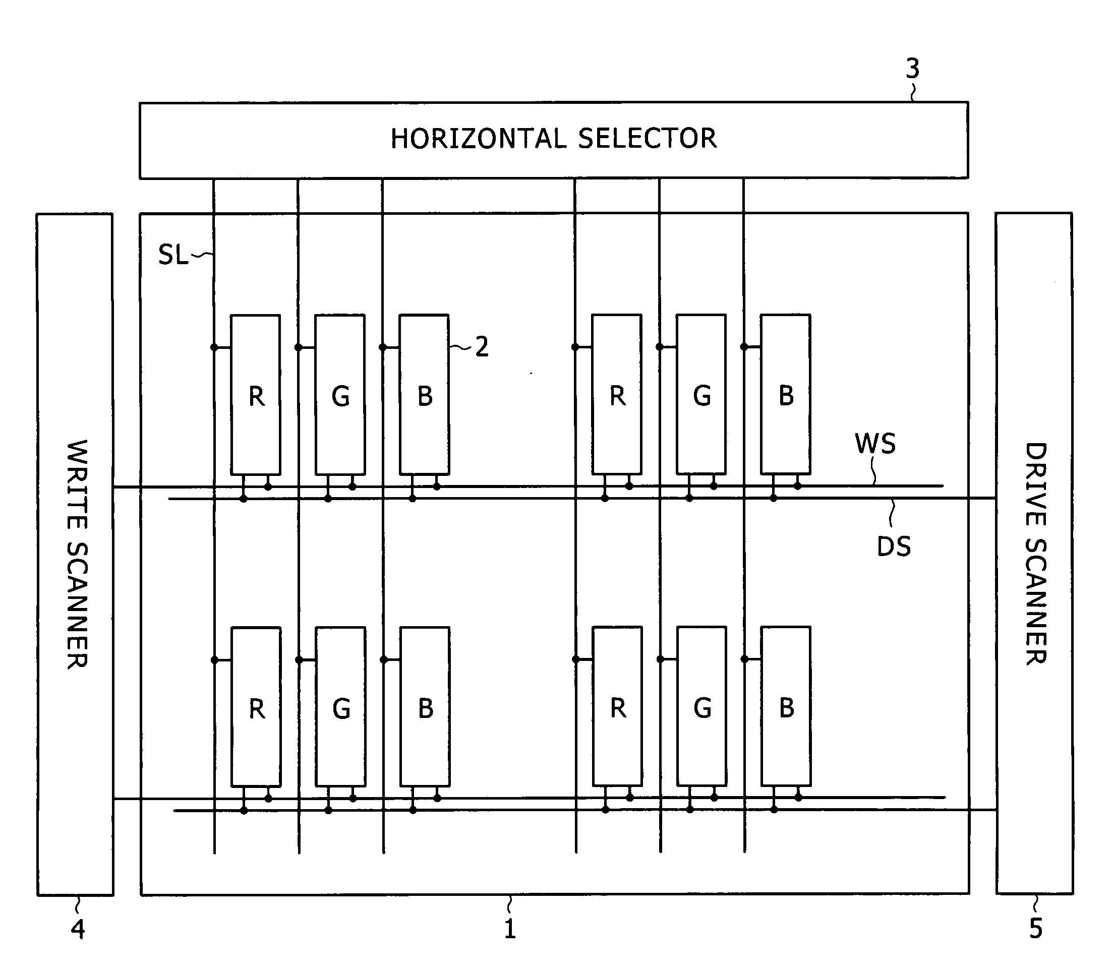
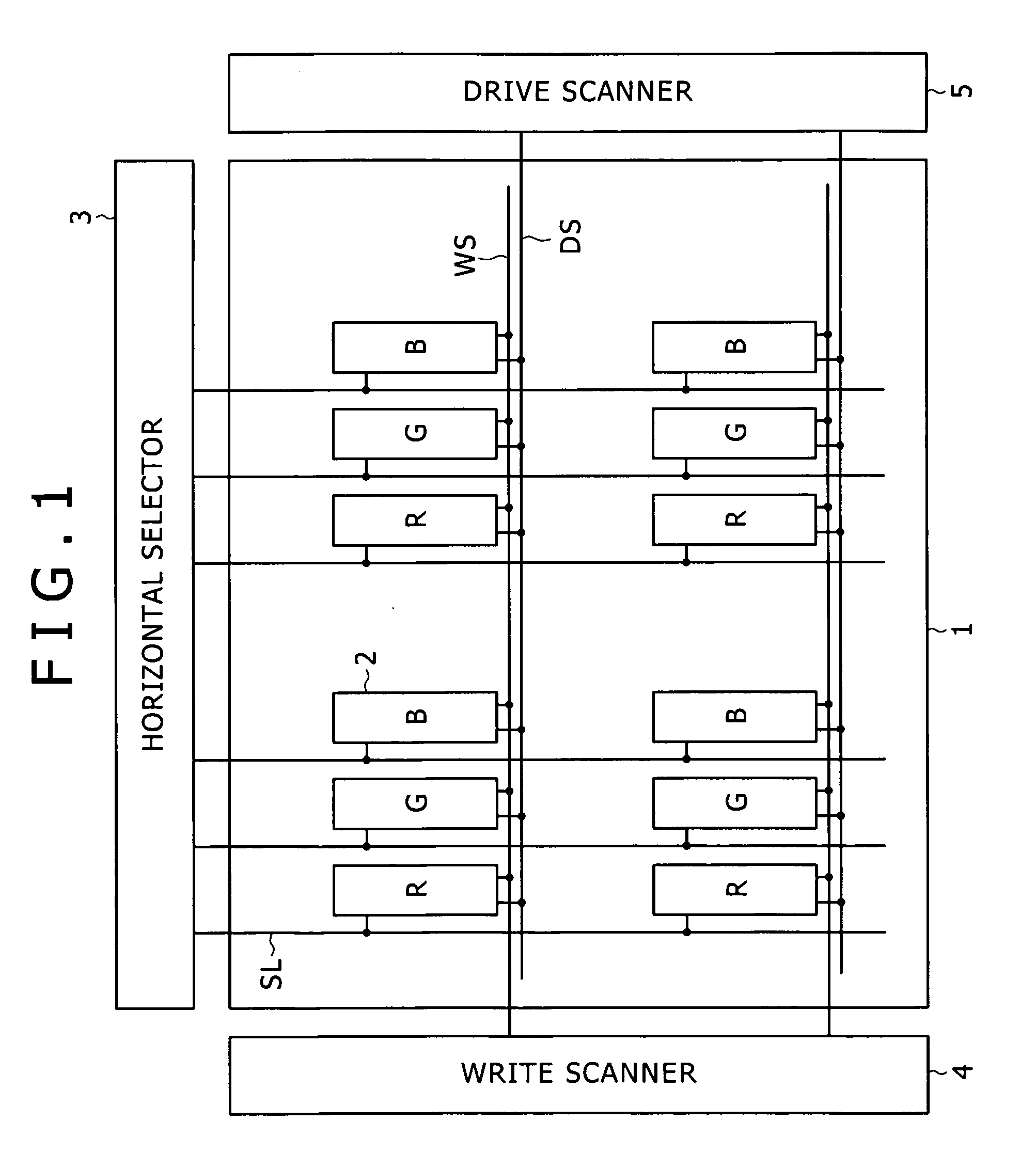
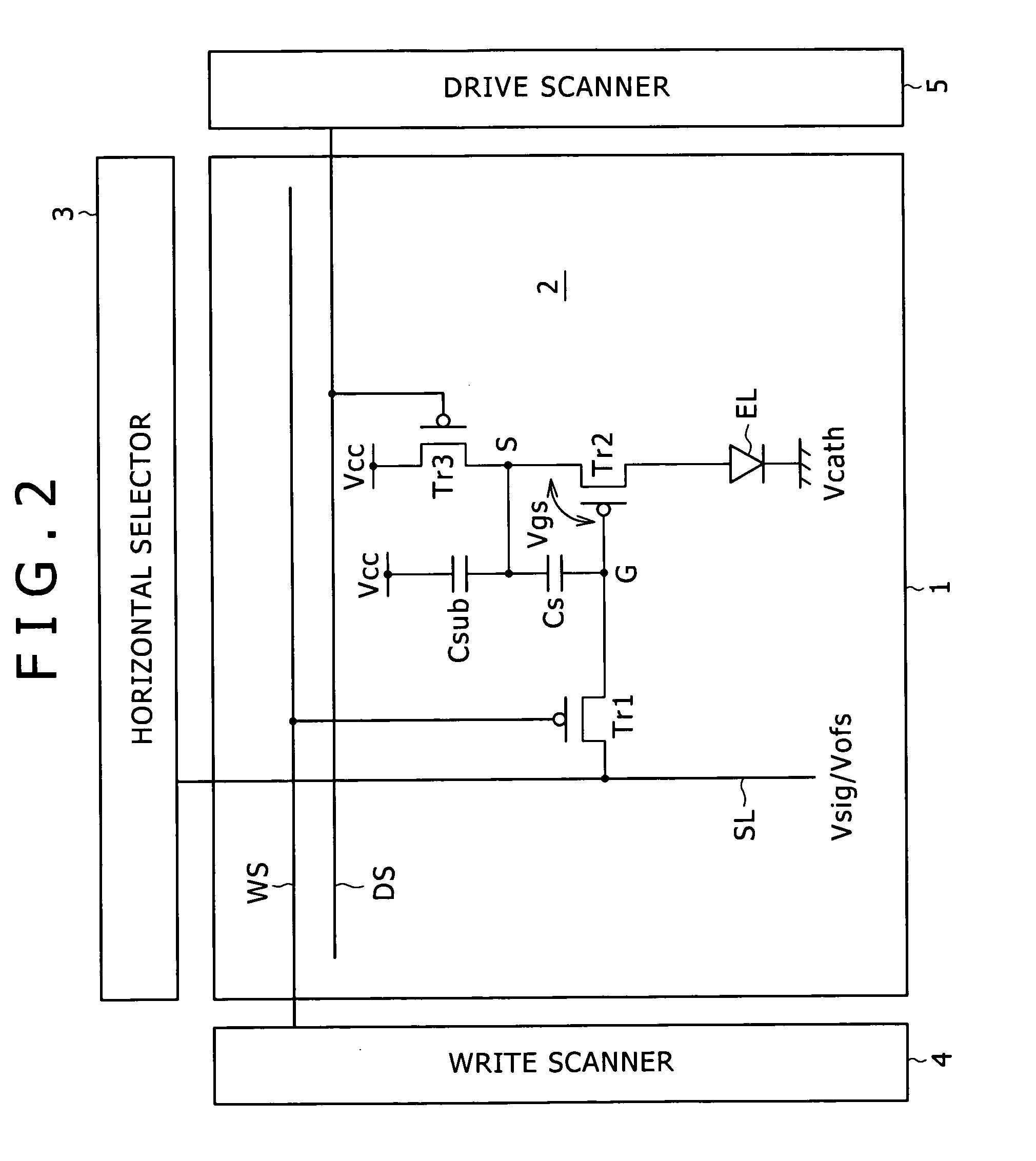
[0041]Preferred embodiments of the present invention will be described in detail with reference to the drawings hereinafter. FIG. 1 is a block diagram showing a general configuration of a display device according to the present invention. As shown in FIG. 1, the display device includes a pixel array unit 1 and a driving unit for driving the pixel array unit 1. The pixel array unit 1 includes first scanning lines WS in the form of rows, second scanning lines DS similarly in the form of rows, signal lines SL in the form of columns, and pixels 2 in the form of a matrix, which pixels are disposed at parts where the scanning lines WS and the signal lines SL intersect each other. Incidentally, in the present example, one of three RGB primary colors is assigned to each of the pixels 2, thus enabling a color display. However, the display device is not limited to this, and it includes a monochrome display panel. The driving unit includes: a write scanner 4 for performing line-sequential driv...

second embodiment

[0067]A display device according to the present invention will be described next. This embodiment can variably adjust a mobility correcting time t automatically according to the level of signal potential.

[0068]FIG. 8 is a graph showing the relation between a signal potential and an optimum mobility correcting time. The y axis indicates the signal potential, and the x axis indicates the optimum mobility correcting time. In a case where a drive transistor Tr2 is of the P-channel type, as in the present invention, the driving current is increased and the light emission luminance is heightened as the signal potential becomes lower. Hence, the light emission luminance changes from a white level through a gray level to a black level as the signal potential is shifted upward. As is clear from the graph, the optimum mobility correcting time tends to be relatively short when the signal potential is at the white level, and tends to be contrarily long when the signal potential is at the black ...


PUM


Abstract

Disclosed herein is a display device including: a pixel array unit; and a driving unit; wherein said pixel array unit includes first scanning lines and second scanning lines in a form of rows, signal lines in a form of columns, and pixels in a form of a matrix, each pixel includes a drive transistor, a sampling transistor, a switching transistor, a retaining capacitance, and a light emitting element, said driving unit includes a write scanner for sequentially supplying a control signal to each first scanning line, a drive scanner for sequentially supplying a control signal to each second scanning line, and a signal selector for alternately supplying a signal potential as a video signal and a predetermined reference potential to each signal line.

Description

CROSS REFERENCES TO RELATED APPLICATIONS[0001]The present invention contains subject matter related to Japanese Patent Application JP 2007-133864 filed in the Japan Patent Office on May 21, 2007, the entire contents of which are incorporated herein by reference.BACKGROUND OF THE INVENTION[0002]1. Field of the Invention[0003]The present invention relates to an active matrix type display device using a light emitting element in a pixel, a driving method thereof, and an electronic device including this kind of display device.[0004]2. Description of the Related Art[0005]A display device, for example, a liquid crystal display, has a large number of liquid crystal pixels arranged in the form of a matrix, and displays an image by controlling the transmission intensity or reflection intensity of incident light in each pixel according to image information to be displayed. This is true for an organic EL display or the like using an organic EL element in a pixel. However, unlike the liquid cry...

Claims


Application Information

Patent Timeline
Patent Type & Authority Applications(United States)
IPC IPC(8): G06F3/038G09G3/34
CPCG09G3/3233G09G2300/0426G09G2300/0439G09G2320/043G09G2300/0814G09G2300/0819G09G2300/0852G09G2300/0443G09G3/002H10K50/11
Inventor YAMASHITA, JUNICHIUCHINO, KATSUHIDE
Owner JOLED INC
Why Eureka
Try Eureka