Electronic device and manufacturing method of electronic device

Inactive Publication Date: 2008-12-04
FUJITSU LTD
View PDF5 Cites 5 Cited by
  • Summary
  • Abstract
  • Description
  • Claims
  • Application Information

AI Technical Summary

Benefits of technology

[0033]According to the present invention, when the second terminal conductor on which the Au plating layer of the second terminal is formed is pressed against and heated with the solder bump precoating the first terminal conductor of the first terminal so as to carry out melting and joint, solder enters the solder joint observation window formed in the second terminal conductor as a notch or a slit so as to form a fillet, the formation state of the solder fillet with respect to the solder joint observation window of the second terminal conductor can be checked from outside via the second insulating layer in an examination step after the solder joint, the joint by an appropriate solder amount that does not protrudes from the second terminal conductor to the outside and has been conventionally considered as an appearance defective product since no protruding part is confirmed can be correctly determined as an appearance non-defective product, and the manufacturing yield can be improved by improving the appearance examination performance.
[0034]The solder enters the notch or a slit formed in the second terminal conductor as a solder joint observation window and forms the solder fillet; therefore, three-dimensional joint is added to

Problems solved by technology

When the cleaning is not perfect, failure due to the flux residue may be caused, and a cleaning process having an enough margin planed when flux is used.
However, when the protruding parts of the solder cannot be observed even when the suspension terminal 110 is viewed like FIG. 2A, even if an appropriate

Method used


Image

  • Electronic device and manufacturing method of electronic device
  • Electronic device and manufacturing method of electronic device
  • Electronic device and manufacturing method of electronic device

Examples


Example

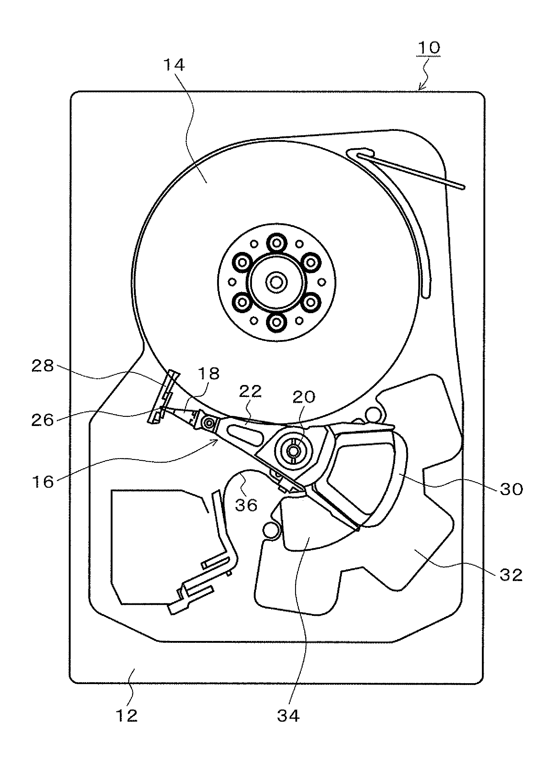
[0064]FIG. 3 is an explanatory drawing which takes a magnetic disk apparatus as an example and shows, as an electronic device of the present invention, an inner structure of a chassis base side by removing a chassis cover. In FIG. 3, in the magnetic disk apparatus 10, a magnetic disk 14 which is rotated at a constant speed by a spindle motor is provided in the chassis base 12. With respect to the magnetic disk 14, a rotary actuator 16 is provided. The rotary actuator 16 is rotatably supported by a shaft unit 20 with respect to the chassis base 12, a head gimbal assembly 18 is attached to the distal end side thereof via an arm 22 so as to support a head 26, and a coil 30 is attached to the rear end side thereof. In the coil 30 side of the rotary actuator 16, a magnetic circuit unit which is fixed to the chassis base 12 is provided, and the coil 30 and the magnetic circuit unit constitute a voice coil motor which drives the rotary actuator 16. In the magnetic circuit unit in the chass...


PUM


Abstract

In the state in which a FPC terminal conductor precoated with a solder bump is opposed to a suspension terminal conductor having an Au plating layer, heating and melting is carried out while the suspension terminal conductor is pressed against the solder bump by a heater chip, thereby joining the FPC terminal conductor with the suspension terminal conductor by solder without using flux. In the suspension terminal conductor, a notch, a slit, or the like is formed as a solder joint observation window through which the solder joint state by the solder bump can be visually checked from outside via an insulating layer.

Description

[0001]This application is a priority based on prior application No. JP 2007-144562, filed May 31, 2007, in Japan.BACKGROUND OF THE INVENTION[0002]1. Field of the Invention[0003]The present invention relates to an electronic device having a structure, in which terminals on each of which a plurality of terminal conductors are arranged on an insulating layer are mutually joined by soldering, and a manufacturing method of the electronic device and, particularly, relates to the electronic device, in which the terminals are mutually joined by soldering without using flux, and a manufacturing method of the electronic device.[0004]2. Description of the Related Arts[0005]Conventionally, as electrical connection between a suspension terminal of a head gimbal assembly which is a component part of a hard disk drive and a base terminal of a flexible printed board on which a head IC is mounted, a method of mutually joining Au terminals by ultrasonic waves is known; and, recently, a method of prec...

Claims


Application Information

Patent Timeline
IPC IPC(8): G11B7/00
CPCH05K1/0269H05K1/056H05K3/363H05K2201/0108H05K2201/09381H05K2201/0969H05K2203/0278H05K2203/163G11B5/4846G11B21/02G11B33/12H05K1/02H05K1/00
Inventor TANAKA, HISAOSHIMOURA, SEIICHI
Owner FUJITSU LTD
Why Eureka
Try Eureka