
Data processing apparatus and data processing method

a data processing apparatus and data processing technology, applied in the field of data processing apparatus and data processing method, can solve the problems of large time, inability to link design data to pattern inspection apparatus, and inability to use tools which link design data to inspection apparatus, etc., to facilitate the tuning of inspection conditions in inspection apparatus, facilitate the cooperation of inspection apparatus, and facilitate the effect of review sem

Inactive Publication Date: 2008-12-04
HITACHI HIGH-TECH CORP
View PDF12 Cites 15 Cited by
  • Summary
  • Abstract
  • Description
  • Claims
  • Application Information

AI Technical Summary

Benefits of technology

[0013]The present invention has been made in view of the above-described problems, and an object thereof is to provide means for comparing the hot spots found by simulation with inspection data of a semiconductor pattern inspection apparatus, and an inspection work support system having a function capable of improving the convenience in use and early displaying a clue to clearing up the cause as an apparatus for outputting coordinate data of the hot spots to a review SEM, automatically arranging SEM images and images output from various inspection apparatuses, and determining inspection conditions or analyzing the instrumental error between apparatuses.
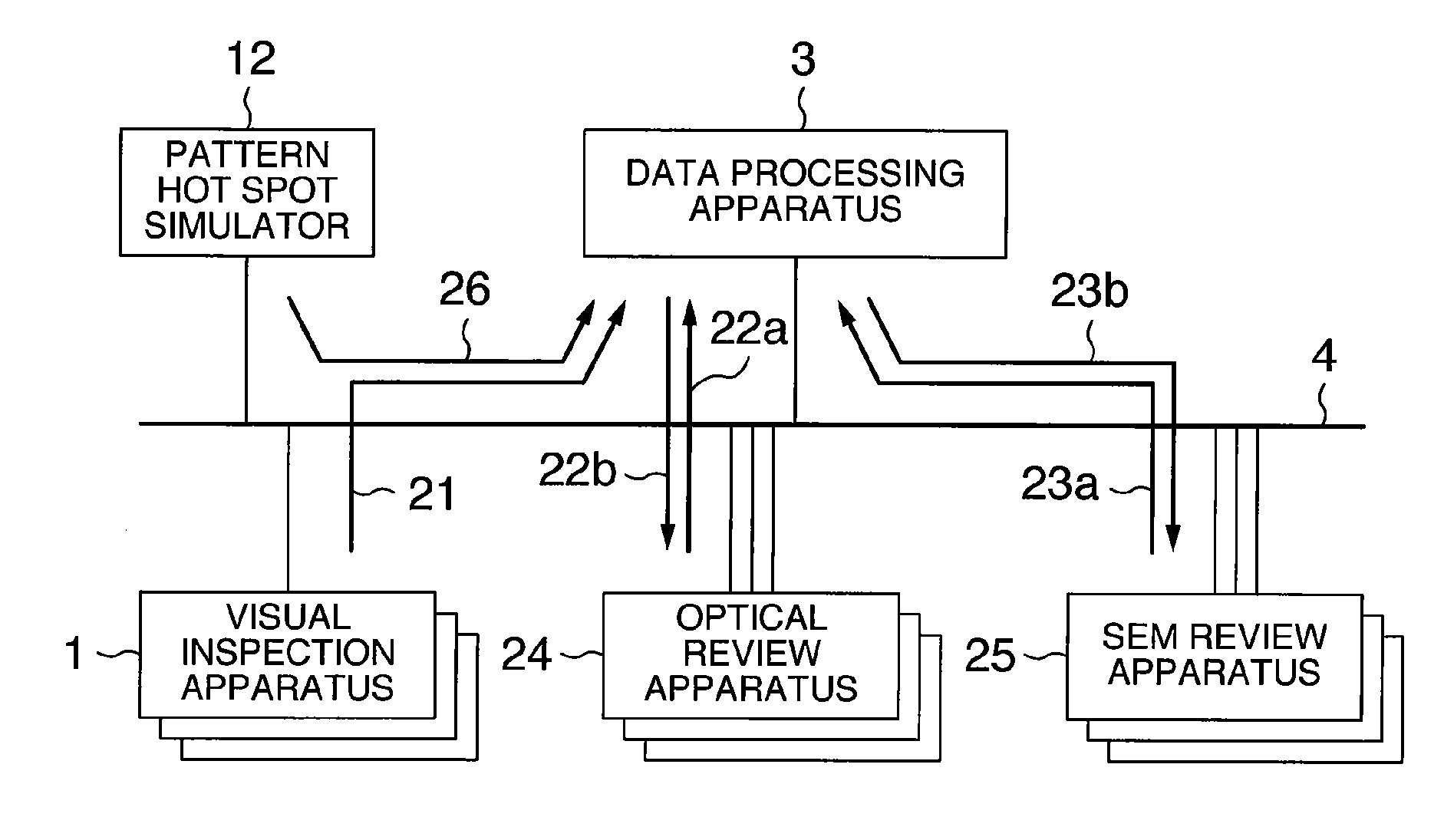
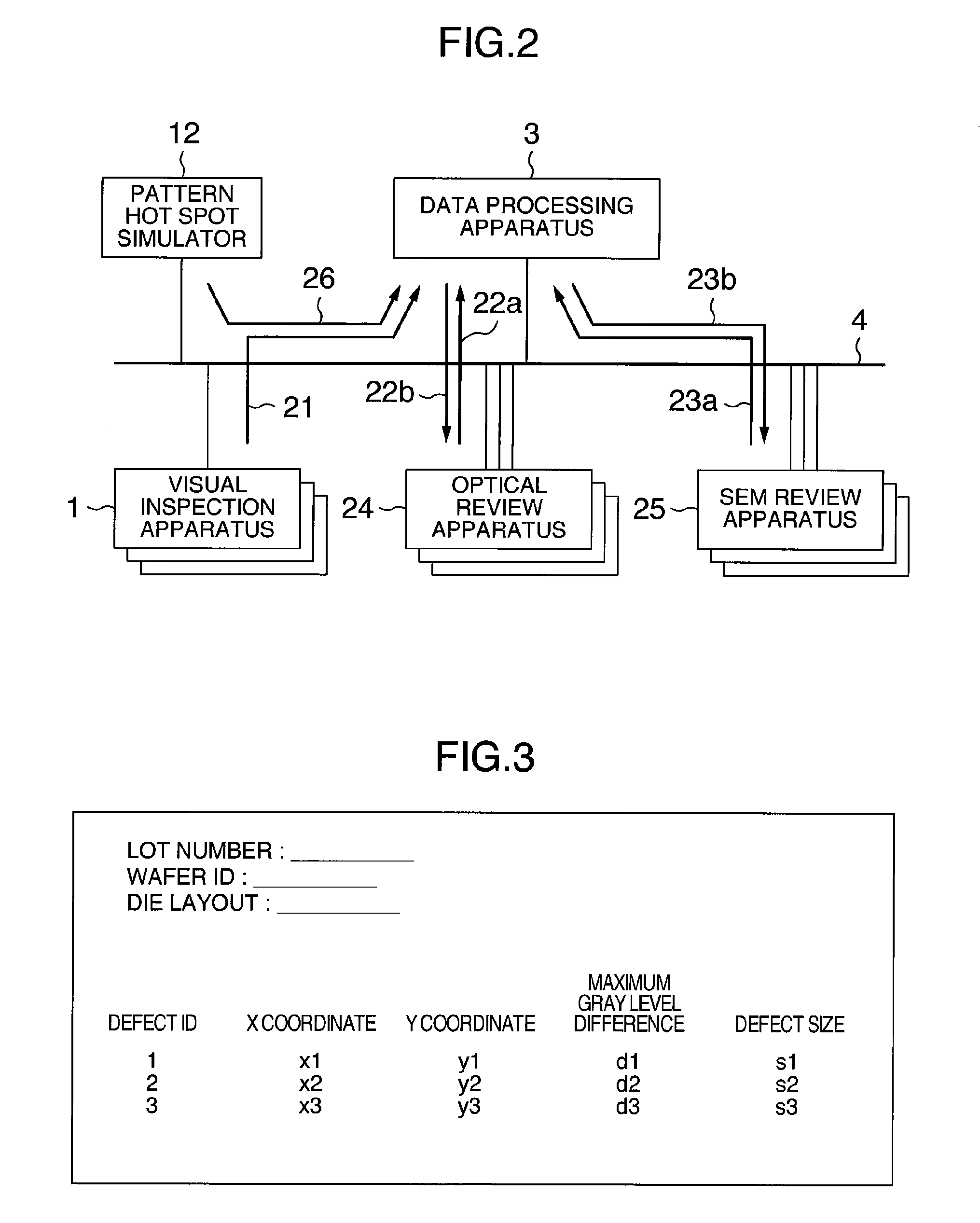
[0014]The object can be achieved by a data processing method comprising the steps of causing a visual inspection apparatus to acquire a plurality of pieces of defect information including defect location coordinates which indicate locations of defects and defect attributes which indicate attributes of the defects obtained by inspecting an inspection subject a plurality of times; causing a pattern hot spot simulator to calculate coordinate data of the hot spots by using a pattern layout stored in a CAD server; causing the pattern hot spot simulator to output the defect location coordinates, the defect attributes, and the coordinate data of the hot spots to a review apparatus; causing the review apparatus to acquire review image information of regions including the defect location coordinates; extracting pattern layout data corresponding to regions including the hot spots on the basis of the coordinate data of the hot spots; storing the plurality of pieces of defect information, the review image information, and the pattern layout data in a data processing apparatus; causing a data processing apparatus to arrange and store each of the defect information, the review image information, and the pattern layout data so as to associate it with the defect location coordinates; and displaying the arranged and stored data on a screen.
[0016]According to the present invention, tuning of inspection conditions in the inspection apparatus is facilitated from a view point of the detection rate of the hot spots. In addition, it is made possible to easily implement a fixed point observation function in a conventional review SEM by outputting coordinate data which can be read by the review SEM. As a result, cooperation among simulation data, the inspection apparatus, and the review SEM can be facilitated.
[0017]According to the present invention, selection of an inspection condition under which the detection rate of the hot spots is high is facilitated by arranging the CAD information and the SEM images side by side and comparing coordinates of inspection data under a plurality of inspection conditions at the same time. As a result, time required until the inspection condition in the inspection apparatus is optimized from a viewpoint of optimization of the detection rate of the hot spots can be reduced remarkably. Eventually, the yield on the line can be improved in a short period of time.

Problems solved by technology

When running the system which compares a pattern image at an image pickup position determined from design data with a system image representing design data as described above in an actual semiconductor manufacture site, the required time is proportionate to the number of acquired images and in general enormous time is needed.
However, there are no tools which link design data to the pattern inspection apparatus.
Furthermore, even if it is attempted to execute the optimization, it takes enormous time.
Therefore, it is unreasonable to run the system in the actual semiconductor manufacture site.
There is no means for optimizing the inspection condition of the semiconductor pattern inspection apparatus for the hot spot found by simulation.
Thus, it is difficult to implement such running.

Method used


Image

  • Data processing apparatus and data processing method
  • Data processing apparatus and data processing method
  • Data processing apparatus and data processing method

Examples


Embodiment Construction

[0028]Hereafter, an embodiment of the present invention will be described in detail with reference to the drawings.

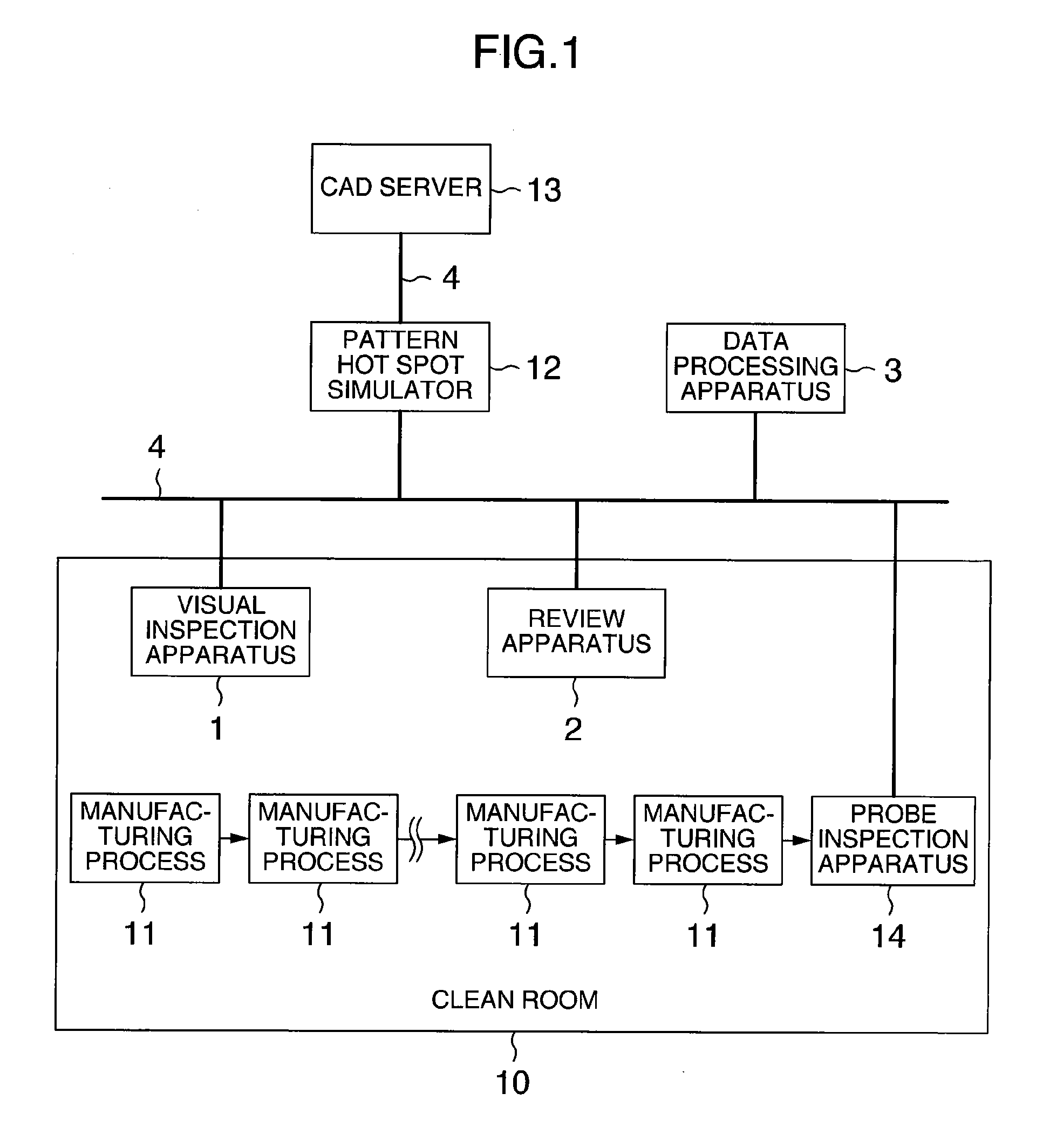
[0029]FIG. 1 is a general configuration diagram including a data processing apparatus according to the present invention. An example in which the data processing apparatus is applied to a semiconductor manufacturing line is shown. Semiconductor manufacturing processes 11 are typically executed in a clean room 10 in which a clean environment is maintained. A visual inspection apparatus 1 for detecting visual defects of product wafers, and a review apparatus 2 for observing, i.e., reviewing visual defects on the basis of data supplied from the visual inspection apparatus are installed in the clean room 10. The visual inspection apparatus 1 and the review apparatus 2 are linked to a data processing apparatus 3 for exchanging inspection and image data and a pattern hot spot simulator 12 via a communication line 4. Product wafers with a lot as the unit flow through the semic...


PUM


Abstract

A data processing apparatus according to the present invention takes in a plurality of inspection, image and attribute data output from an inspection apparatus, a review SEM image, coordinate information of hot spots found by simulation, and CAD information in the hot spots, and displays these kinds of information side by side. Tuning of inspection conditions in the inspection apparatus is facilitated from a view point of the detection rate of the hot spots. In addition, it is made possible to easily implement a fixed point observation function in a conventional review SEM by outputting coordinate data which can be read by the review SEM. Cooperation among simulation data, the inspection apparatus, and the review SEM is facilitated.

Description

BACKGROUND OF THE INVENTION[0001]The present invention relates to a data processing apparatus, and data processing method. In particular, the present invention relates to a data processing apparatus, and data processing method which supports condition determining work and analysis for confirming apparatus performance in an apparatus for detecting particles and pattern defects on the surface of a semiconductor wafer, a photomask, a magnetic disk, a liquid crystal substrate or the like, and an observation apparatus for observing defects such as particles.[0002]In the semiconductor manufacturing process, particles and pattern defects on the wafer surface cause defects in products. Therefore, it is necessary to quantify the particles and pattern defects (hereafter referred to as visual defects) and always monitor whether there is a problem in a manufacturing apparatus and a manufacturing environment. In addition, it is necessary to confirm whether a visual defect exerts a fatal influenc...

Claims


Application Information

Patent Timeline
IPC IPC(8): G06K9/00
CPCG01N21/9501G01N21/95607G01N2021/8864G01N2021/95615
Inventor FUNAKOSHI, TOMOHIROHIJIKATA, SHIGEAKI
Owner HITACHI HIGH-TECH CORP
Learn More