Array of small contacts for solar cell fabrication

a solar cell and contact technology, applied in the field of solar cells, can solve the problems of limiting the processing parameters of other steps in the back end process, contact masks typically require critical alignment,

Active Publication Date: 2008-12-04
MAXEON SOLAR PTE LTD
View PDF32 Cites 43 Cited by
  • Summary
  • Abstract
  • Description
  • Claims
  • Application Information

AI Technical Summary

Benefits of technology

[0007]These and other features of the present invention will be readily apparent to persons of ordinary skill in the art upon reading the entirety of this disclosure, which includes the accompanying drawings and claims.

Problems solved by technology

However, the contact mask typically requires critical alignment with other features of the solar cell wafer.
This alignment limits the processing parameters of other steps in the back end process.

Method used


Image

  • Array of small contacts for solar cell fabrication
  • Array of small contacts for solar cell fabrication
  • Array of small contacts for solar cell fabrication

Examples


Embodiment Construction

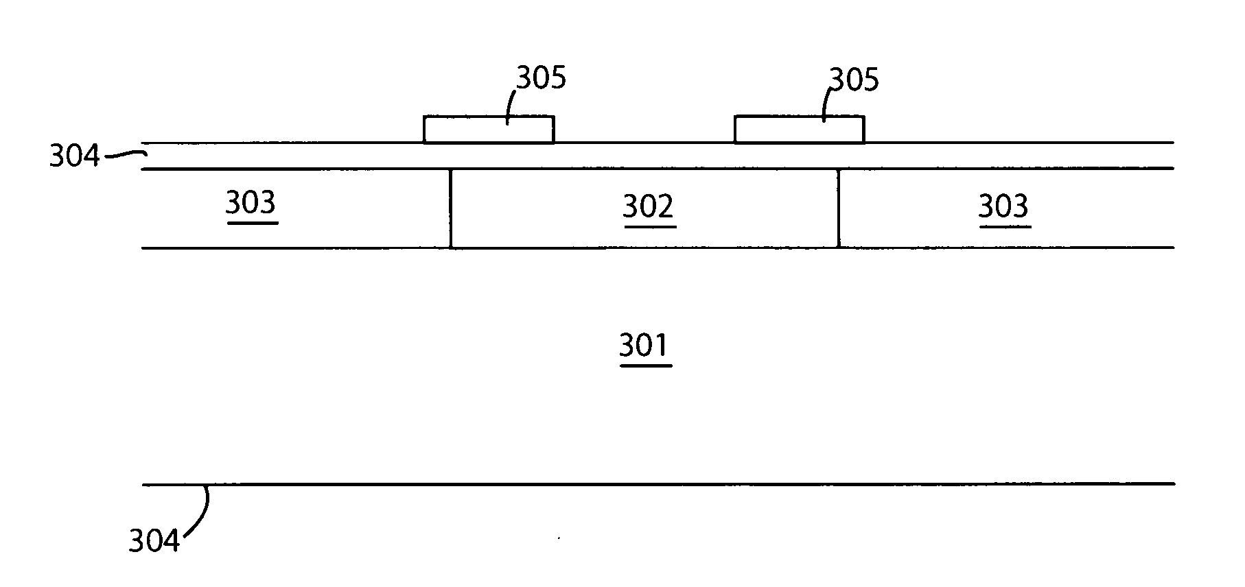
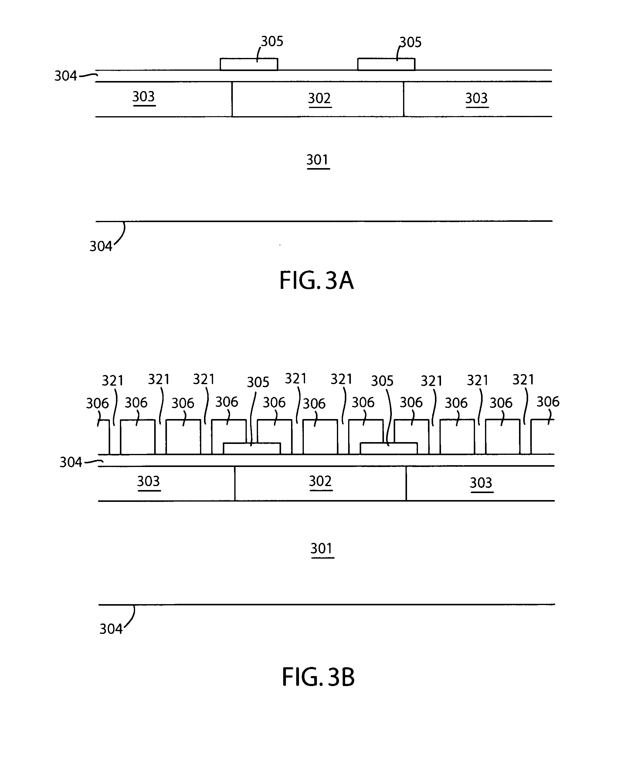
[0014]In the present disclosure, numerous specific details are provided, such as examples of apparatus, structures, and methods, to provide a thorough understanding of embodiments of the invention. Persons of ordinary skill in the art will recognize, however, that the invention can be practiced without one or more of the specific details. In other instances, well-known details are not shown or described to avoid obscuring aspects of the invention.

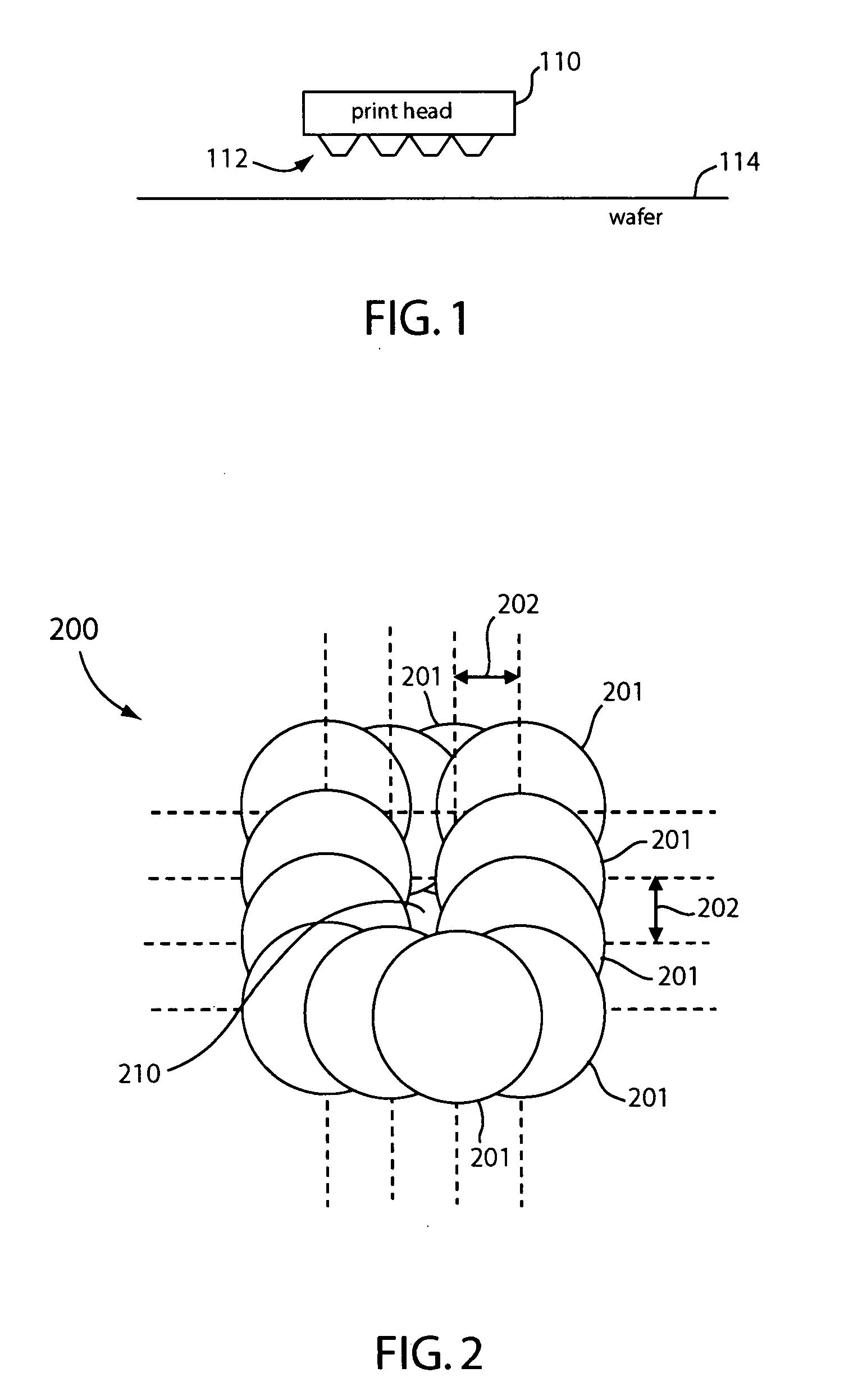
[0015]FIG. 1 schematically shows an example inkjet printer that may be used in embodiments of the present invention. In the example of FIG. 1, the inkjet printer includes a printhead 110 and a plurality of nozzles 112. The nozzles 112 may be arranged in rows and columns to form an array. The use of inkjet printers in semiconductor processing, in general, is well known. Briefly, material is flowed through the nozzles 112 and onto a wafer 114. One or more passes of the printhead 110 over the wafer 114 results in a pattern being printed on the...


PUM


Abstract

Fabrication of a solar cell using a printed contact mask. The contact mask may include dots formed by inkjet printing. The dots may be formed in openings between dielectric layers (e.g., polyimide). Intersections of overlapping dots may form gaps that define contact regions. The spacing of the gaps may be dictated by the alignment of nozzles that dispense the dots. Using the dots as a contact mask, an underlying dielectric layer may be etched to form the contact regions through the underlying dielectric layer. Metal contact fingers may be formed over the wafer to form electrical connections to corresponding diffusion regions through the contact regions.

Description

BACKGROUND OF THE INVENTION[0001]1. Field of the Invention[0002]The present invention relates generally to solar cells, and more particularly but not exclusively to solar cell fabrication processes and structures.[0003]2. Description of the Background Art[0004]Solar cells are well known devices for converting solar radiation to electrical energy. They may be fabricated on a semiconductor wafer using semiconductor processing technology. Generally speaking, a solar cell may be fabricated by forming P-type and N-type diffusion regions in a silicon substrate. Solar radiation impinging on the solar cell creates electrons and holes that migrate to the diffusion regions, thereby creating voltage differentials between the diffusion regions. In a backside junction solar cell, both the diffusion regions and the metal contact fingers coupled to them are on the backside of the solar cell. The contact fingers allow an external electrical circuit to be coupled to and be powered by the solar cell....

Claims


Application Information

Patent Timeline
Patent Type & Authority Applications(United States)
IPC IPC(8): B05D5/12
CPCH01L21/0337H01L21/31144H01L21/76802Y02E10/547H01L31/022441H01L31/0682H01L31/022425H01L31/04
Inventor COUSINS, PETER JOHNCUDZINOVIC, MICHAEL JOSEPH
Owner MAXEON SOLAR PTE LTD
Why Eureka
Try Eureka