
Light emitting device and method for manufacturing the same
- Summary
- Abstract
- Description
- Claims
- Application Information
AI Technical Summary
Benefits of technology
Problems solved by technology
Method used
Image

Examples
first embodiment
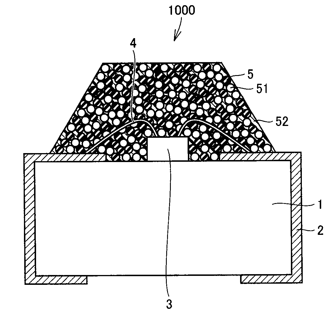
[0074]FIG. 1 is a schematic cross-sectional view showing a light emitting device of the present invention. Referring to FIG. 1, the following description will be given. A light emitting device 1000 is provided with a substrate 1, patterned wires 2 formed on substrate 1, a light emitting element 3 mounted on substrate 1, bonding wires 4 used for electrically connecting patterned wires 2 and light emitting element 3 to each other, and a mold component used for sealing these. The mold component includes phosphor particles 5, resin particles 51 and a sealing resin 52. Light emitting element 3, which has P-side electrodes and N-side electrodes (not shown) formed on its one of the faces, is electrically connected to patterned wires 2 by two bonding wires, with the corresponding face serving as an upper face.
[0075]In the description of the present invention, “particles” mean grain-shaped particles, and resin particles 51 and phosphor particles 5 are preliminarily formed into grain shapes. ...
second embodiment
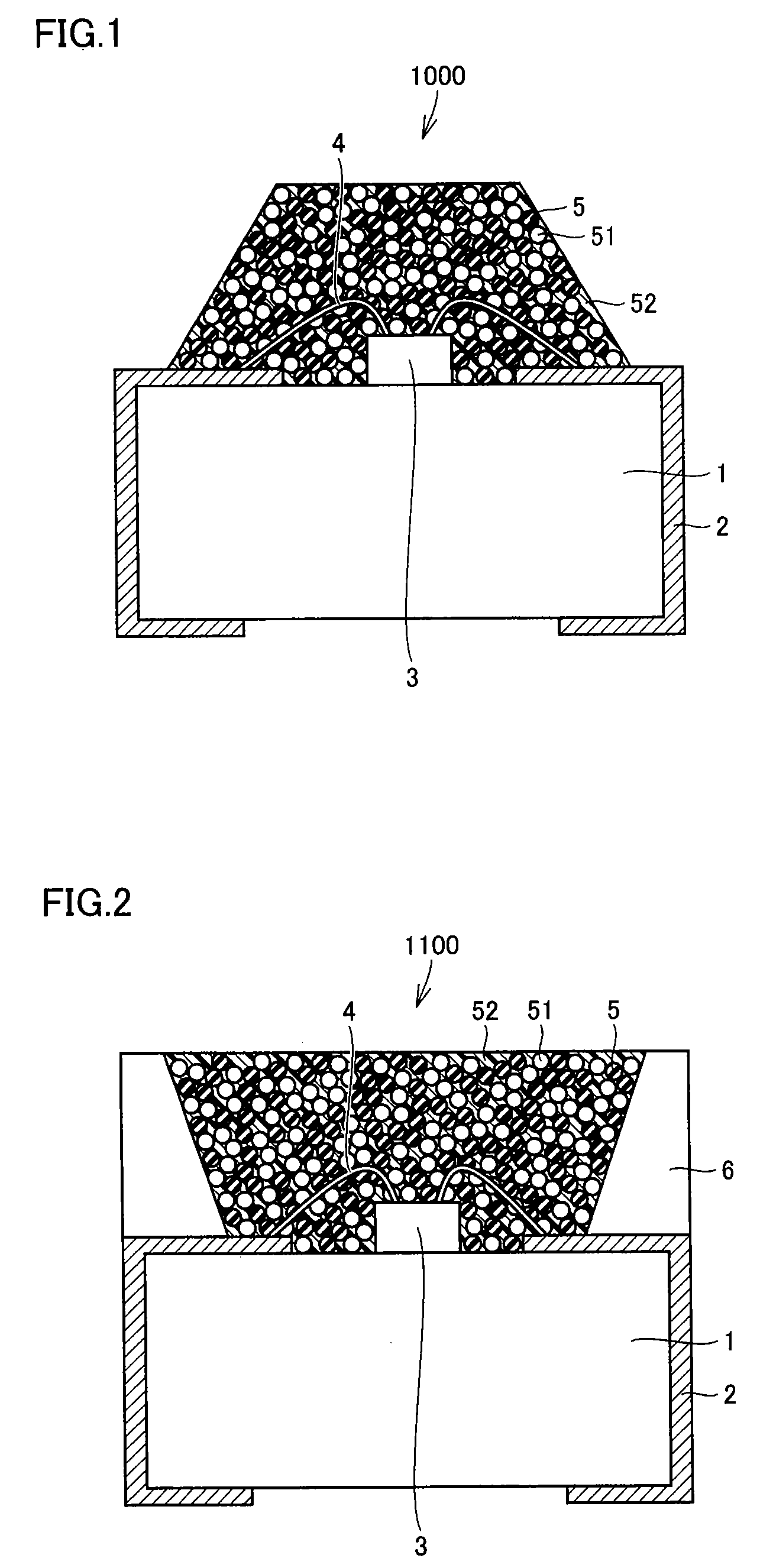
[0101]FIG. 2 is a schematic cross-sectional view showing another light emitting device of the present invention. Referring to FIG. 2, the following description will be given. A light emitting device 1100 is basically provided with a substrate 1, patterned wires 2 formed on substrate 1, a light emitting element 3, bonding wires 4 used for electrically connecting patterned wires 2 and light emitting element 3 to each other, a mold component used for sealing these and a reflector frame 6 that reflects light. The mold component includes phosphor particles 5, resin particles 51 and a sealing resin 52.
[0102]The present embodiment has the same structure as that of the first embodiment except that it is provided with a reflector frame 6. Reflector frame 6 is allowed to reflect light efficiently from a slanted face made in contact with the mold component, and thus has a function for releasing light externally from the light emitting device. Moreover, reflector frame 6 also has a function for...
third embodiment
[0120]FIG. 9 is a schematic cross-sectional view showing still another light emitting device of the present invention. Referring to FIG. 9, the following description will be given. A light emitting device 1400 is basically provided with a substrate 1, patterned wires 2 formed on substrate 1, a light emitting element 3, bonding wires 4 used for electrically connecting patterned wires 2 and light emitting element 3 to each other, a mold component used for sealing these and a reflector frame 6 that reflects light. The mold component includes phosphor particles 5, resin particles 51 and a sealing resin 52.
[0121]The present embodiment has the same structure as that of the second Embodiment except that the mold component has a laminated-layer structure in which layers of resin particles 51 and layers of phosphor particles 5 are alternately laminated in a thickness direction. It should be noted that, with respect to the layers of resin particles 51 and the layers of phosphor particles 5, t...
PUM
| Property | Measurement | Unit |
|---|---|---|
| Thickness | aaaaa | aaaaa |
| Particle size | aaaaa | aaaaa |
| Refractive index | aaaaa | aaaaa |
Abstract
Description
Claims
Application Information