Field effect transistor using carbon based stress liner

a stress liner and field effect technology, applied in the direction of transistors, semiconductor devices, electrical equipment, etc., can solve the problems of decreasing the effectiveness of stress liner, increasing the difficulty of trend continuation,

Inactive Publication Date: 2008-12-11
GLOBALFOUNDRIES INC
View PDF10 Cites 43 Cited by
  • Summary
  • Abstract
  • Description
  • Claims
  • Application Information

AI Technical Summary

Benefits of technology

[0022]A particular semiconductor structure in accordance with the invention includes a field effect device including a gate electrode located over a channel region within a semiconductor substrate that separates a pair of source / drain regions within the semiconductor substrate. This particular semiconductor structure also includes a stress liner located over the field effect device. The stress liner includes a carbon based material.
[0023]Another particular semiconductor structure in accordance with the invention also includes a field effect device including a gate electrode located over a channel region within a semiconductor substrate that separates a pair of source / drain regions within the semiconductor substrate. This other particular semiconductor structure also includes a stress liner located over the field effect device. The stress liner includes at least one of a dielectric material and a semiconductor material having a stress greater than about 5 GPa.
[0024]Yet another particular semiconductor structure in accordance with the invention also includes a field effect device including a gate electrode located over a channel region within a semiconductor substrate that separates a pair of source / drain regions within the semiconductor substrate. This other particular semiconductor structure also includes a stress liner located over the field effect device. The stress liner has a dielectric constant less than about 7.
[0025]A particular method for fabricating a semiconductor structure in accordance with the invention includes forming within and upon a semiconductor substrate a field effect device including a gate electrode formed over a channel region within the semiconductor substrate that separates a pair of source / drain regions formed within the semiconductor substrate. This particular method also includes forming a carbon based stress liner over the field effect device.

Problems solved by technology

This trend is becoming increasingly more difficult to continue as the devices reach their physical scaling limits.
However, as gate pitch dimensions decrease, effectiveness of stress liners, including in particular silicon nitride stress liners, decreases.

Method used


Image

  • Field effect transistor using carbon based stress liner
  • Field effect transistor using carbon based stress liner
  • Field effect transistor using carbon based stress liner

Examples


Embodiment Construction

[0031]The invention, which includes a semiconductor structure that includes a field effect device that includes a stress liner comprising a stress liner material that has particular dielectric constant and stress properties that may be realized within the context of a particular stress liner material, is understood within the context of the description set forth below. The description set forth below is understood within the context of the drawings described above. Since the drawings are intended for illustrative purposes, the drawings are not necessarily drawn to scale.

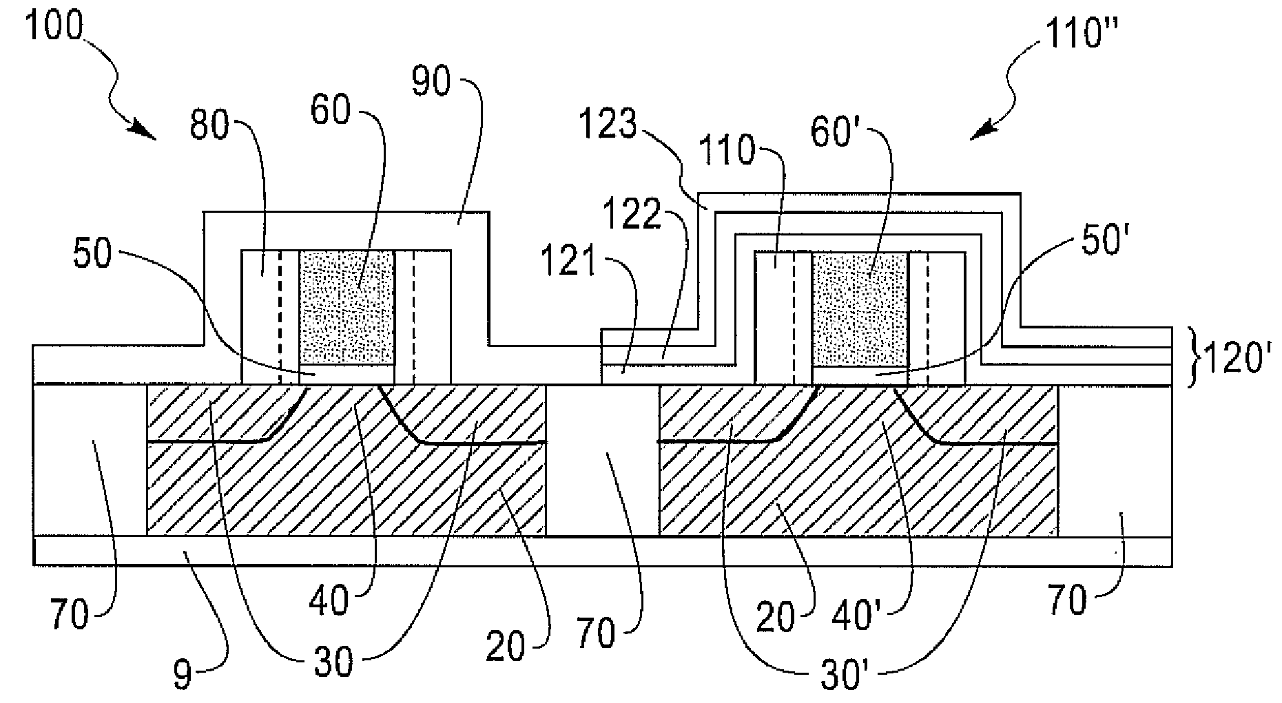
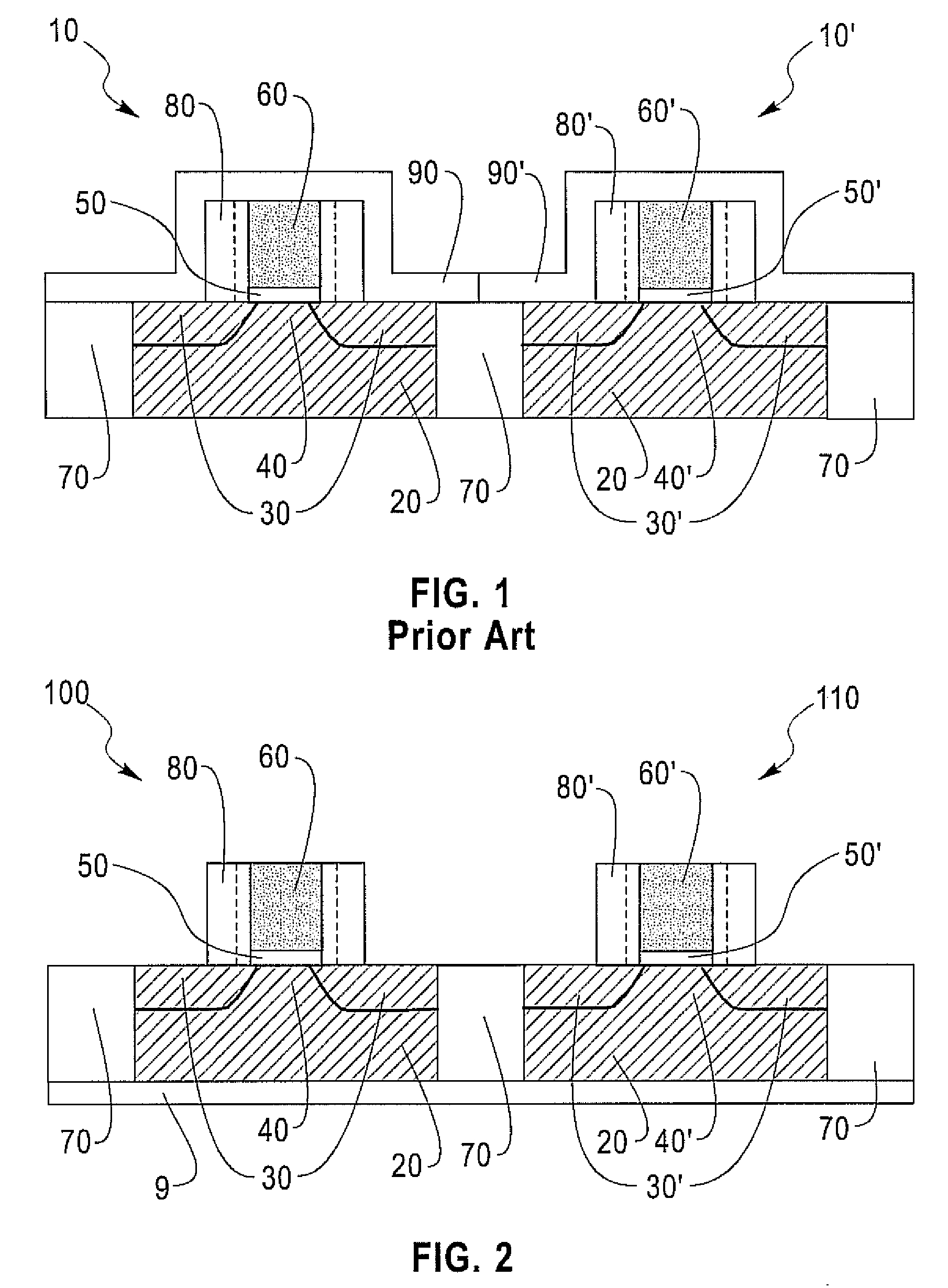
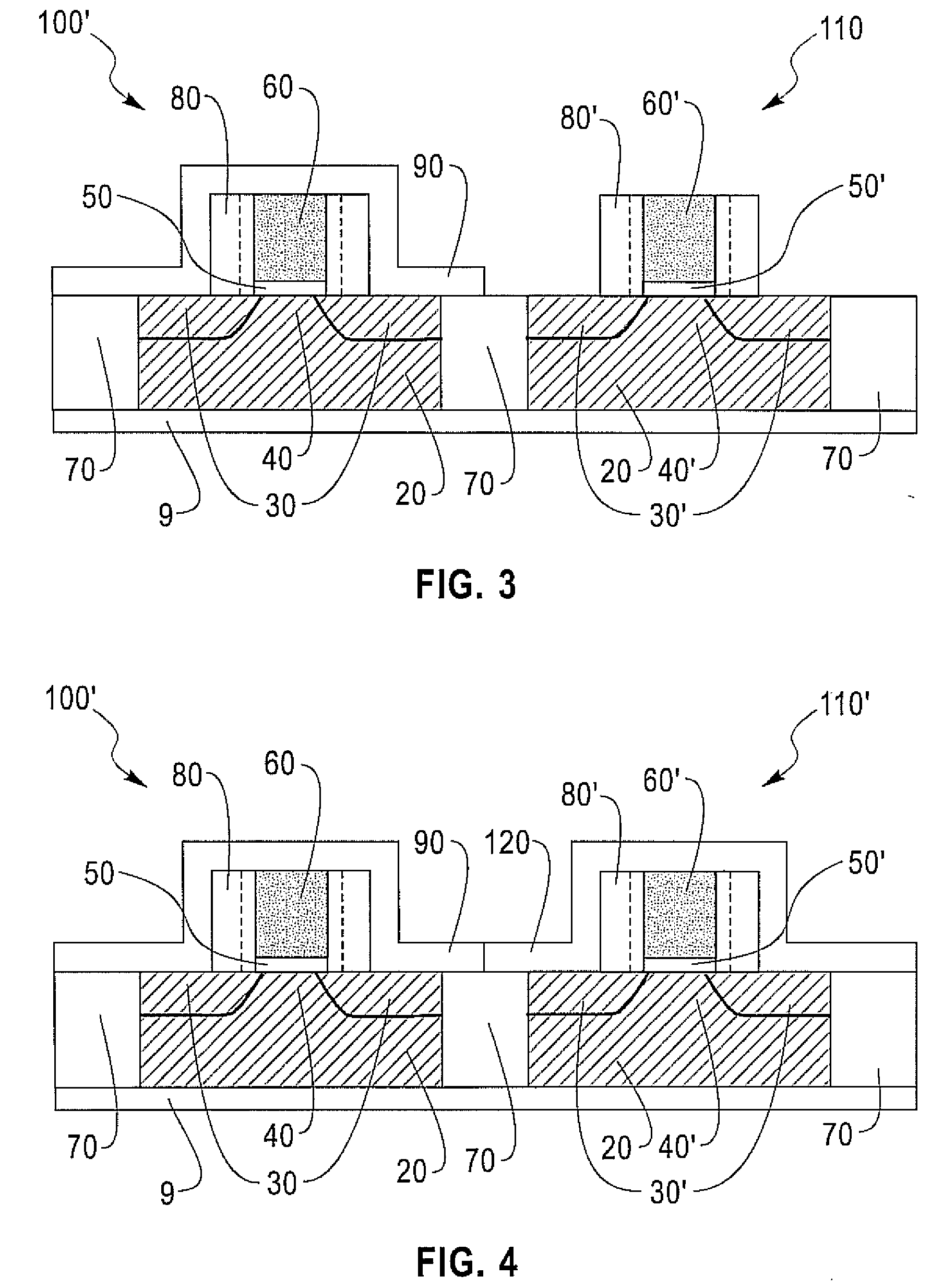
[0032]FIG. 2 to FIG. 4 show a series of schematic cross-sectional diagrams illustrating the results of progressive stages in fabricating a CMOS structure in accordance with an embodiment of the invention. This particular embodiment of the invention comprises a first embodiment of the invention. FIG. 2 shows a schematic cross-sectional diagram of the CMOS structure at an early stage in the fabrication thereof in accor...


PUM

PropertyMeasurementUnit
dielectric constantaaaaaaaaaa

Abstract

A stress liner for use within a semiconductor structure that includes a field effect device has a dielectric constant less than about 7 and a compressive stress greater than about 5 GPa. The stress liner may be formed of a carbon based material, preferably a tetrahedral amorphous carbon (ta-C) material including at least about 60 atomic percent carbon and no greater than C about 40 atomic percent hydrogen. The carbon based material may be either a dielectric material, or given appropriate additional dielectric isolation structures, a semiconductor material. In particular, a ta-C stress liner may be formed using a filtered cathodic vacuum arc (FCVA) physical vapor deposition (PVD) method.

Description

BACKGROUND[0001]1. Field of the Invention[0002]The invention relates generally to channel stress within field effect devices. More particularly, the invention relates to stress liners that influence channel stress within field effect devices.[0003]2. Description of the Related Art[0004]Historically, most performance improvements in semiconductor field effect transistor (FET) devices have been realized by a downward scaling of the relative dimensions of the devices. This trend is becoming increasingly more difficult to continue as the devices reach their physical scaling limits. As a consequence, advanced FETs and the complementary metal oxide semiconductor (CMOS) circuits in which they may be used, are increasingly utilizing strain engineering to achieve desired circuit performance.[0005]Strain engineering relies on the observation that carrier mobility within a semiconductor channel of a field effect device may be increased by inducing a mechanical strain within the semiconductor c...

Claims


Application Information

Patent Timeline
Patent Type & Authority Applications(United States)
IPC IPC(8): H01L29/78H01L21/336
CPCH01L21/823807H01L27/092H01L29/665H01L29/6659H01L29/7833H01L29/7843
Inventor GRILL, ALFREDNGUYEN, SONSAENGER, KATHERINE L.
Owner GLOBALFOUNDRIES INC
Why Eureka
Try Eureka