Radiation detecting apparatus and radiographing system
- Summary
- Abstract
- Description
- Claims
- Application Information
AI Technical Summary
Benefits of technology
Problems solved by technology
Method used
Image
Examples
first embodiment
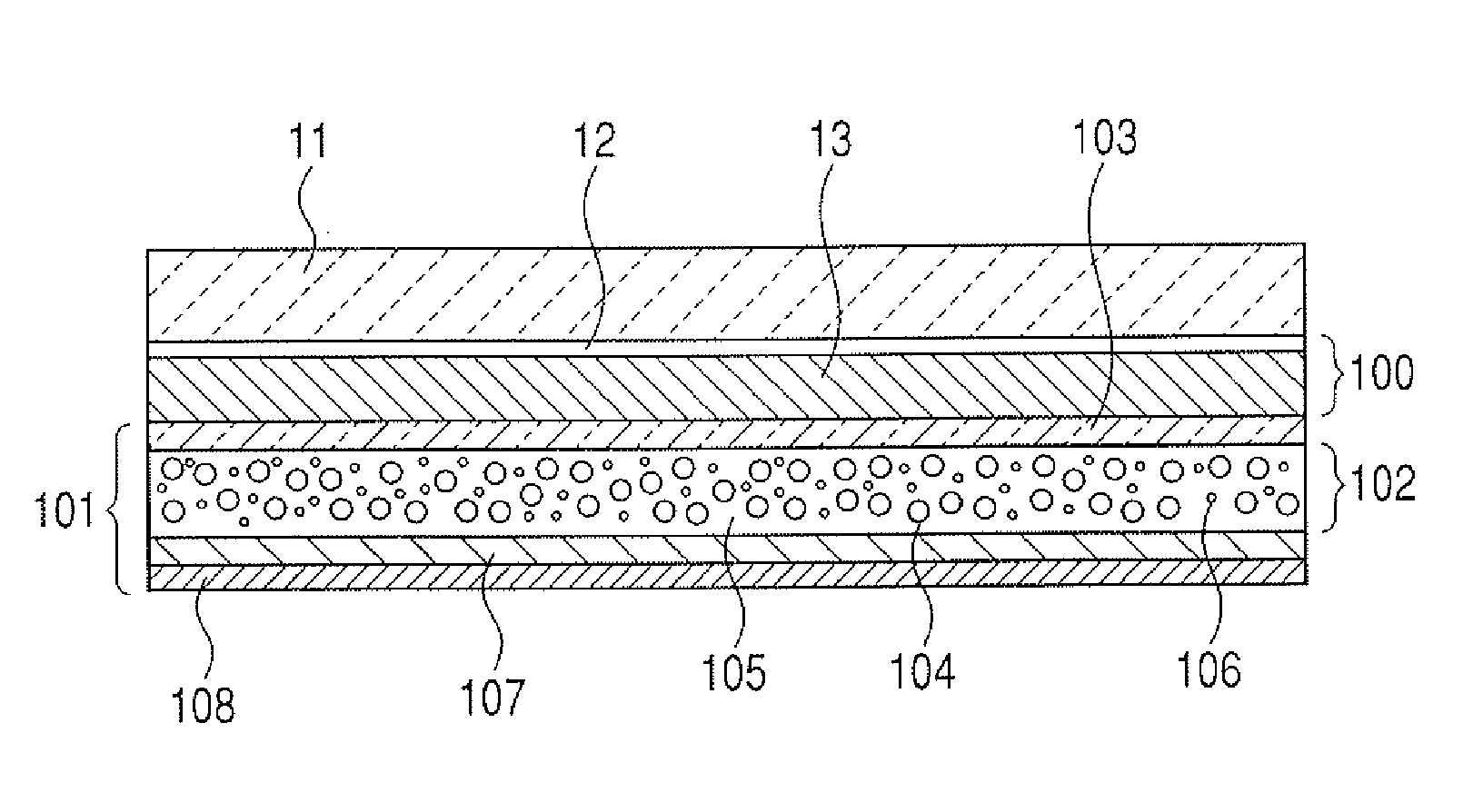
[0039]FIG. 1 is a cross-sectional view of the radiation detecting apparatus according to this embodiment. As shown in FIG. 1, the light emitting unit 101, the sensor panel 100, and the scintillator layer 11 being CsI (Tl) on the sensor panel are arranged in the apparatus. The black pigment 106 is dispersed in the light emitting layer 102 of the light emitting unit 101. The black pigment 106 is carbon black; specifically, channel black is used herein. The light emitting unit 101 can radiate light to at least a light reception range of the photoelectric conversion element array 12. The black pigment 106 efficiently absorbs light transmitting the substrate 13 from the sensor panel by light emission from the scintillator layer, so that a trace amount of components are reflected on the photoelectric conversion element array 12 of the sensor panel 100. The black pigment 106 also absorbs light from the light emitting unit 101. As such, the amount of light emission from the light emitting u...
second embodiment
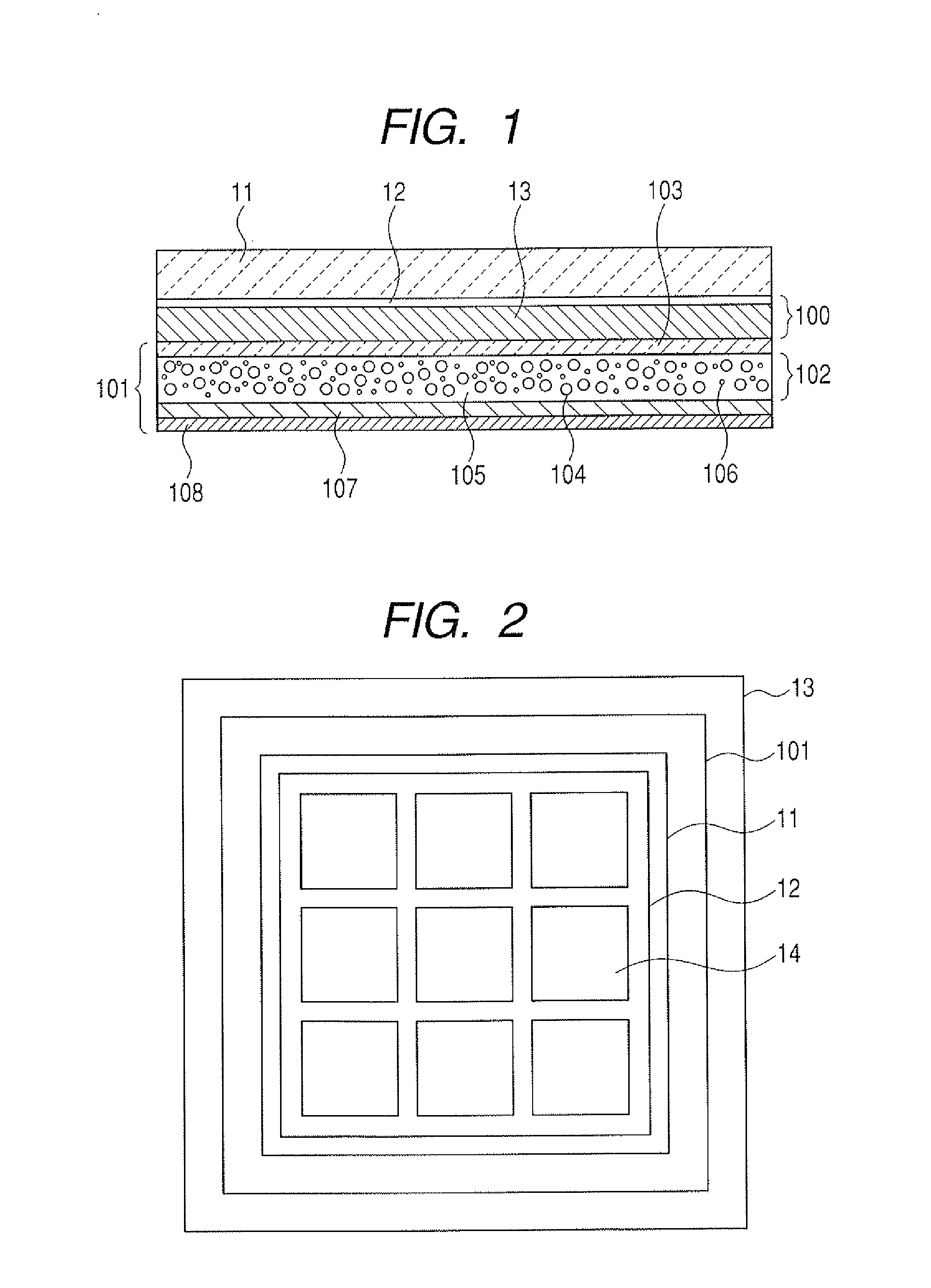
[0043]FIG. 3 is a cross-sectional view of a radiation detecting apparatus according to this embodiment. As shown in FIG. 3, the light emitting unit 101, the sensor panel 100, and the scintillator layer 11 being CsI (Tl) are arranged in the apparatus, similarly to the first embodiment. Differently from the first embodiment, the light emitting layer 102 does not contain a black pigment, but contains purple and red pigments. That is, the light emitting layer 102 of the light emitting unit 101 contains two kinds of pigments 109. In that case, the layer 102 containing the two kinds of pigments 109 also absorbs light from the light emitting unit 101. However, the amount of light emission from the light emitting unit is larger than the light transmitting the substrate 13 from the sensor panel by light emission from the scintillator layer. In the above manner, light necessary for optical calibration can transmit the apparatus, thereby reducing reflected light inducing degradation of the ima...
third embodiment
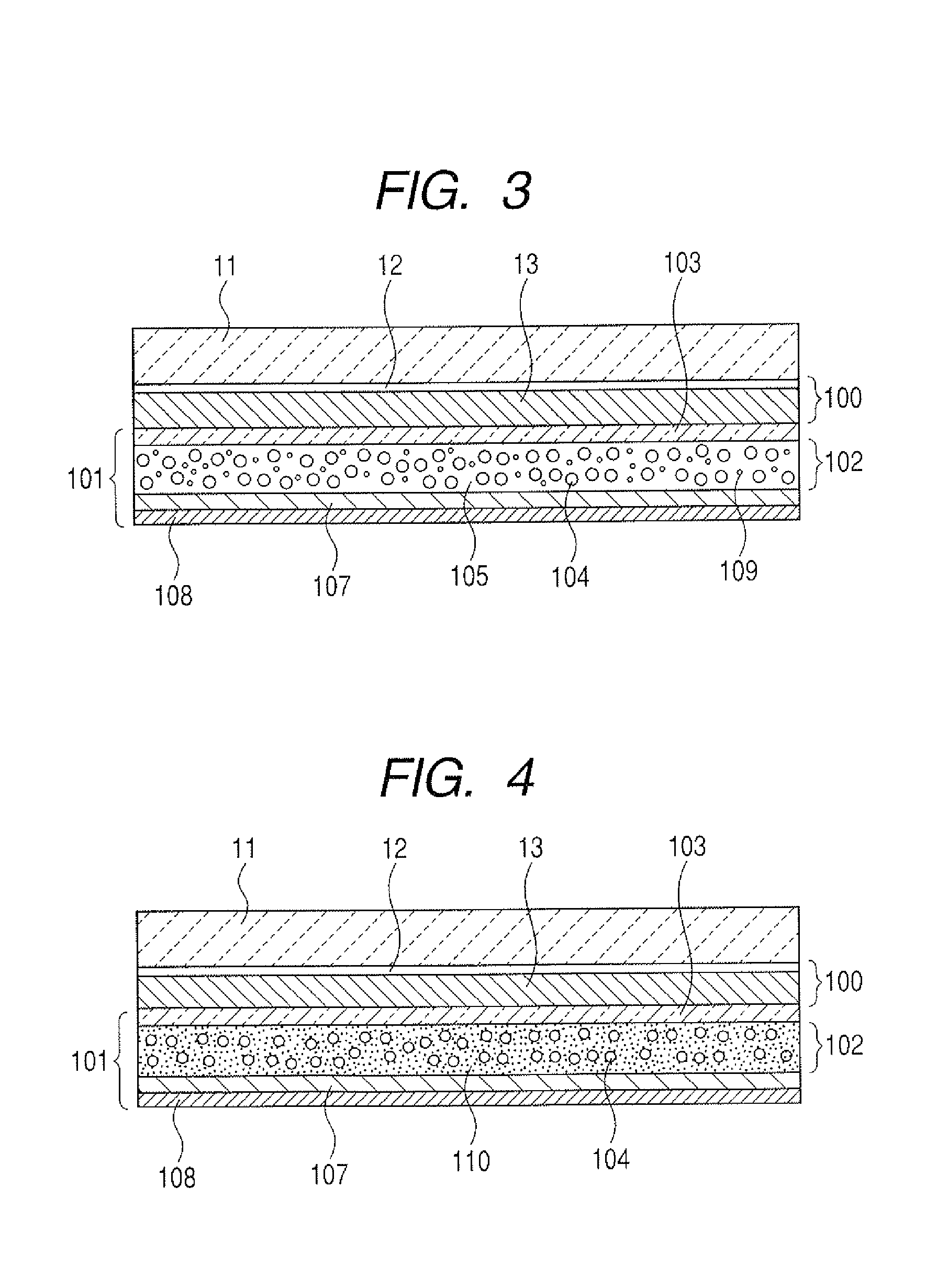
[0045]FIG. 4 is a cross-sectional view of a radiation detecting apparatus according to this embodiment. As shown in FIG. 4, the light emitting unit 101, the sensor panel 100, and the scintillator layer 11 being CsI (Tl) are arranged in the apparatus, similarly to the second embodiment. Differently from the second embodiment, the light emitting layer 102 does not contain pigments but contains dyes. The dyes are purple and red similarly to the second embodiment. As such, the light emitting layer 102 of the light emitting unit 101 includes the light emitting substance 104 and a binder 110 containing dyes. The binder is colored by the dyes so that the colored binder efficiently absorbs light transmitting the substrate 13 from the sensor panel by light emission from the scintillator layer. Accordingly, a trace amount of components are reflected on the photoelectric conversion element array 12 of the sensor panel 100. The binder 110 containing dyes also absorbs light from the light emitti...
PUM
 Abstract
Description
Claims
Application Information
 - R&D Engineer
- R&D Manager
- IP Professional
- Industry Leading Data Capabilities
- Powerful AI technology
- Patent DNA Extraction
Browse by: Latest US Patents, China's latest patents, Technical Efficacy Thesaurus, Application Domain, Technology Topic, Popular Technical Reports.
© 2024 PatSnap. All rights reserved.Legal|Privacy policy|Modern Slavery Act Transparency Statement|Sitemap|About US| Contact US: help@patsnap.com


