Dispaly Pixel Inversion Scheme

a technology of inversion scheme and display device, applied in the field of display device, can solve the problems of biasing electric field across the cell, unsatisfactory biasing electric field, and problem of charge build-up, so as to improve the use of image data analysis results, and disable the second inversion scheme

Inactive Publication Date: 2008-12-18
KONINKLIJKE PHILIPS ELECTRONICS NV
View PDF8 Cites 21 Cited by
  • Summary
  • Abstract
  • Description
  • Claims
  • Application Information

AI Technical Summary

Benefits of technology

[0022]By introducing a step of analyzing the image data, yielding correlation values between frames, it is hence possible to adapt the inversion scheme to the particular type of image data that is currently being displayed. This is advantageous in that it allows changing of the inversion scheme, e.g., only at scene changes in the image sequence and thereby disguising any flickering of the image as perceived by a viewer when the inversion takes place.
[0023]The number of frame periods between two consecutive polarity inversions according to the second scheme may, in an embodiment, be set to an essentially infinite number, thereby essentially disabling the second inversion scheme. This is advantageous if, e.g., it is discovered that the pseudo-random inv

Problems solved by technology

However, during a period of several frame durations a build-up of a biasing charge occurs, resulting in a biasing electric field across the cell.
Such a biasing electric field is not desirable since it will change the transmission characteristics of the cell.
But when such com

Method used


Image

  • Dispaly Pixel Inversion Scheme
  • Dispaly Pixel Inversion Scheme
  • Dispaly Pixel Inversion Scheme

Examples


Embodiment Construction

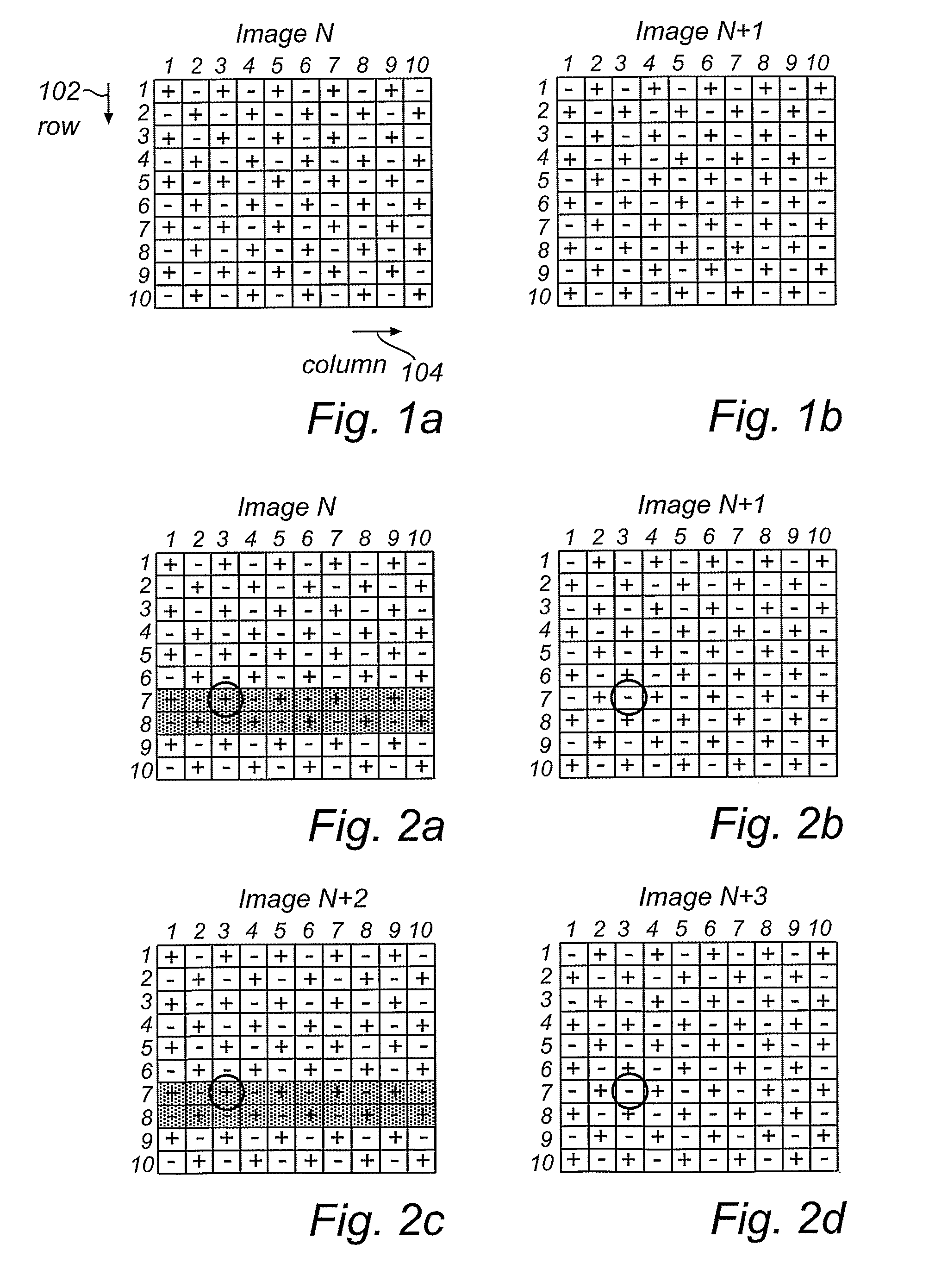
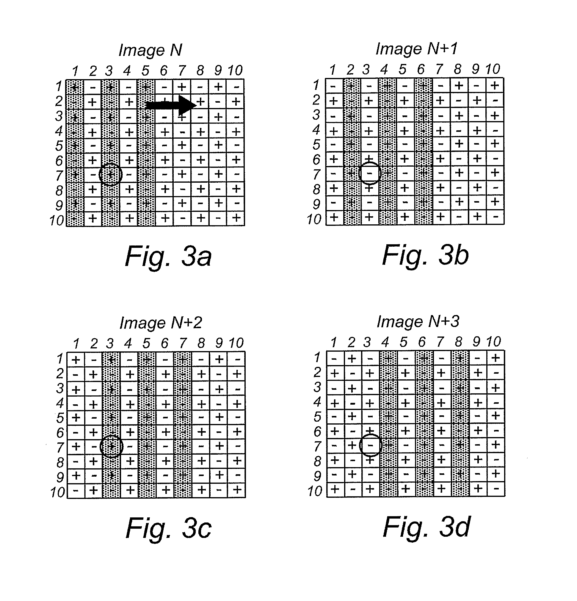
[0031]In what follows, a number of image data frames will be schematically illustrated, comprising 100 picture cells (or pixels) arranged in 10 rows by 10 columns, as indicated by arrows 102, 104 in FIG. 1a. In the image data frames of FIGS. 1 to 4, the picture cells that contain a dotted pattern illustrate bright (as perceived by a viewer) pixels and white cells represent dark pixels. A plus (+) sign represents a positive driving level, i.e. the sum of a common voltage level and a voltage level representing the data of the pixel in the image data signal. A minus (−) sign represents a negative driving level, i.e. the difference between a common voltage level and a voltage level representing the data of the pixel in the image data signal.

[0032]An LCD picture cell changes its transmission depending on the strength of the electric field over the cell, i.e. irrespective of the polarity of the field. A known problem related to LCD's is that a long-term voltage bias results in the cell dr...


PUM


Abstract

A display device (500) having a plurality of picture cells (502) is controlled by adding a phase change to the regular cyclic inversion scheme. Thereby, it is possible to overcome the drawbacks of DC build-up due to, e.g., de-interlaced images and images comprising rotating symbols and “ticker tape”. The control involves receiving an image signal comprising image data relating to the picture cells. A respective electric field across each picture cell is controlled, in dependence on at least the image data, according to a first polarity inversion scheme where the polarity of the electric field is such that polarity inversion occurs at regular intervals, and according to a second polarity inversion scheme concurrent with said first polarity inversion scheme, where the polarity of the electric field such that polarity inversion occurs at pseudo-random intervals.

Description

TECHNICAL FIELD[0001]The present invention relates to a display device and a method of controlling a display device in order to avoid build-up of unwanted electric charges in picture cells of the display device.BACKGROUND[0002]Picture cells in a liquid crystal display (LCD) device obtain their transmission characteristics depending on the strength of the electric field across the cell. The electric field across each cell is depending on the content of an image data signal provided from an image source. The data of the image data signal is temporally arranged in a continuous sequence blocks of image data, where each block of data contains data values for each cell corresponding to voltage values to be applied across each cell at regular refresh intervals. Typically, blocks of image data and refresh intervals are referred to as image frames and frame periods.[0003]In principle, the transmission characteristics of a picture cell is independent of the direction of the electric field acr...

Claims


Application Information

Patent Timeline
IPC IPC(8): G09G5/00G09G3/36
CPCG09G3/3614G09G2320/0204G09G2320/0247G09G3/36H04N5/66
Inventor VAN WOUDENBERG, ROELGROOT HULZE, HENDRIKUS WILLEMHEKSTRA, GERBEN JOHANVAN GORKOM, RAMON PASCALWUBBEN, ROBERTUS HENDRICUS MARIA
Owner KONINKLIJKE PHILIPS ELECTRONICS NV
Why Eureka
Try Eureka