Semiconductor device and manufacturing method thereof

a technology of semiconductor devices and semiconductors, applied in the direction of semiconductor devices, basic electric elements, electrical appliances, etc., can solve the problems of low reliability, difficult to fill the gap with metal films, and titanium films as barrier layers, so as to prevent the generation of aluminum spikes and enhance reliability

Active Publication Date: 2008-12-25
MITSUBISHI ELECTRIC CORP
View PDF3 Cites 33 Cited by
  • Summary
  • Abstract
  • Description
  • Claims
  • Application Information

AI Technical Summary

Benefits of technology

[0016]The present invention was made in view of the above problem, and it is an object of the present invention to provide a semiconductor device capable of enhancing reliability in order to prevent an aluminum spike from generating, and a manufacturing method thereof.

Problems solved by technology

However, according to the constitution and manufacturing method disclosed in the Japanese Patent Laying-Open No. 2002-353456, a fine gap is generated between the filling layer and the trench inner wall, and an aluminum spike is generated at that part, which lowers the reliability.
Therefore, even when a sputtering apparatus used for the most advanced LSI is used, it is extremely difficult to fill this gap with a metal film such as titanium (Ti) film as a barrier layer.
Thus, silicon is diffused in aluminum, and at the same time, aluminum eats away in the silicon as a spike (that is, an aluminum spike is generated), so that the electric characteristics are considerably damaged and long-term reliability cannot be maintained.

Method used


Image

  • Semiconductor device and manufacturing method thereof
  • Semiconductor device and manufacturing method thereof
  • Semiconductor device and manufacturing method thereof

Examples


embodiment 1

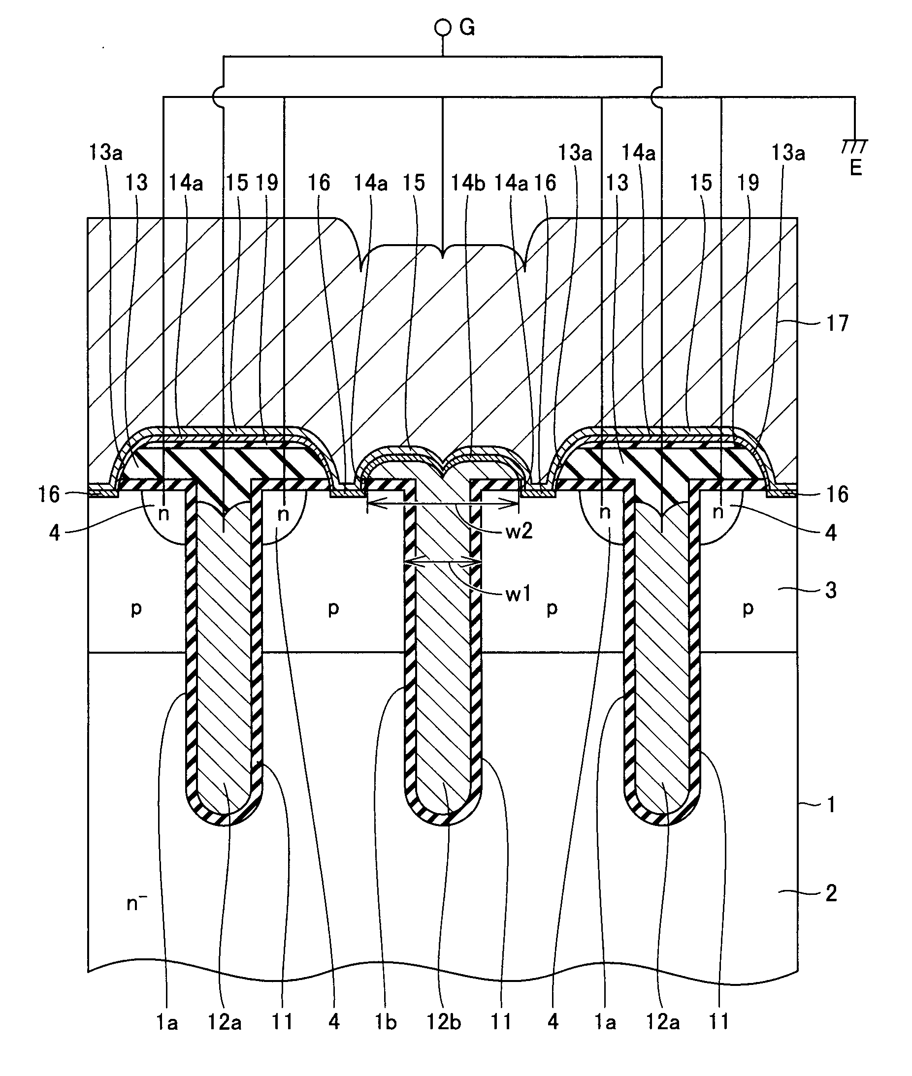
[0037]With reference to FIG. 1, a semiconductor device according to the present embodiment can be applied to a vertical or lateral MOSFET (Metal Oxide Semiconductor Field Effect Transistor), an IGBT and the like.

[0038]Description will be made taking as an example the constitution of an MOS gate part on a surface of the IGBT or MOSFET having a trench gate structure. While an n-channel MOS gate will be taken as an example for convenience of the description, the constitution and effect are the same with the MOS gate of an opposite conductivity type, that is, a p-channel type.

[0039]For example, an n− region 2 serving as a drift region is formed in a semiconductor substrate 1 formed of silicon. A p-type region 3 serving as a base region, for example, is formed on n− region 2 on the first main surface side of semiconductor substrate 1. An n-type region 4 serving as an emitter region (source region) is selectively formed in p-type region 3 on the first main surface side of semiconductor su...

embodiment 2

[0083]The constitution shown in FIG. 1 can be applied to a vertical type IGBT shown in FIGS. 13 to 15, a vertical type n-channel MOSFET (referred to as n-MOSFET hereinafter) shown in FIG. 16, and a lateral type IGBT shown in FIG. 17.

[0084]The vertical type means that a main current flows between electrodes formed on the first and second main surfaces of a semiconductor substrate. Further, the lateral type means that a main current flows between electrodes formed on the first main surface of a semiconductor substrate.

[0085]With reference to FIG. 13, this constitution is in a case where the constitution in FIG. 1 is applied to a vertical PT (Punch Through) type IGBT. In this constitution, n+region (n+ buffer region) 5 and a p+ region (p+ collector region) 6 are sequentially formed on the second main surface side of n− region (n− drift region) 2 of semiconductor substrate 1. A main electrode (collector electrode) 18 is formed on the second main surface of semiconductor substrate 1 so a...

embodiment 3

[0094]While the case where the gate of the insulated gate field effect part has the trench gate structure has been described in Embodiment 1 shown in FIG. 1, the gate of the insulated gate field effect part may have a planar gate structure. Hereinafter, the constitution will be described.

[0095]With reference to FIG. 18, n− region 2 serving as a drift region, for example, is formed in semiconductor substrate 1 formed of silicon. P-type region 3 serving as a base region, for example, is selectively formed on n− region 2 on the first main surface side of semiconductor substrate 1. N-type region 4 serving as an emitter region (source region), for example, is selectively formed in p-type region 3 on the first main surface side of semiconductor substrate 1.

[0096]On the first main surface, gate electrode 12a is formed on p-type region 3 sandwiched between n-type region 4 and n− region 2 through insulation film (gate insulation film) 11. Gate electrode 12a is formed on the flat first main s...


PUM


Abstract

A semiconductor substrate has a trench in a first main surface. An insulated gate field effect part includes a gate electrode formed in the first main surface. A potential fixing electrode fills the trench and has an expanding part expanding on the first main surface so that a width thereof is larger than the width of the trench. An emitter electrode is formed on the first main surface and insulated from the gate electrode electrically and connected to a whole upper surface of the expanding part of the potential fixing electrode. Thus, a semiconductor device capable of enhancing reliability in order to prevent an aluminum spike from generating and a manufacturing method thereof can be provided.

Description

BACKGROUND OF THE INVENTION[0001]1. Field of the Invention[0002]The present invention relates to a semiconductor device and a manufacturing method thereof.[0003]2. Description of the Background Art[0004]As a power semiconductor device as a switching element for driving a motor and the like, an IGBT (Insulated Gate Bipolar Transistor) is mainly used in a region where a regular voltage is 300V or more.[0005]As such a power semiconductor device, a constitution, in which two types of trench inside IGBT cells are provided for both a gate-trench and a non-gate trench filled with a conducting material directly connected to an emitter electrode to have the same potential of emitter region not a gate, has been conventionally proposed (refer to Japanese Patent Laying-Open No. 2002-353456, and Pamphlet of International Publication No. WO 02 / 058160).[0006]Especially, according to the Japanese Patent Laying-Open No. 2002-353456, the gate electrode of the IGBT and the filling layer having the emi...

Claims


Application Information

Patent Timeline
Patent Type & Authority Applications(United States)
IPC IPC(8): H01L29/739H01L21/331
CPCH01L29/0696H01L29/407H01L29/41741H01L29/41766H01L29/456H01L29/7813H01L29/66734H01L29/7393H01L29/7396H01L29/7397H01L29/7455H01L29/66348
Inventor MINATO, TADAHARUTAKANO, KAZUTOYO
Owner MITSUBISHI ELECTRIC CORP
Why Eureka
Try Eureka