Micro-lens fabricated from semiconductor wafer

a technology of semiconductor wafers and micro-lens, applied in the field of micro-lens, can solve the problems of manufacturing lens and external shape, and achieve the effect of simple and highly accurate manner

Inactive Publication Date: 2008-12-25
LAPIS SEMICON CO LTD
View PDF2 Cites 1 Cited by
  • Summary
  • Abstract
  • Description
  • Claims
  • Application Information

AI Technical Summary

Benefits of technology

[0012]The present invention has been carried out under the conditions described above and has a first purpose to provide a method of enabling to assess in a simple and highly accurate manner an amount of misalignment with the optical axis caused by an error in a manufacturing process of a micro-lens.

Problems solved by technology

That is, an error in manufacturing the lens and the external shape of lens are not required to be measured in high accuracy.

Method used


Image

  • Micro-lens fabricated from semiconductor wafer
  • Micro-lens fabricated from semiconductor wafer
  • Micro-lens fabricated from semiconductor wafer

Examples


Embodiment Construction

[0076]In the following detailed description of the preferred embodiments, reference is made to the accompanying drawings which form a part hereof, and in which is shown by way of illustration specific preferred embodiments in which the inventions may be practiced. These preferred embodiments are described in sufficient detail to enable those skilled in the art to practice the invention, and it is to be understood that other preferred embodiments may be utilized and that logical, mechanical and electrical changes may be made without departing from the spirit and scope of the present inventions. The following detailed description is, therefore, not to be taken in a limiting sense, and scope of the present inventions is defined only by the appended claims.

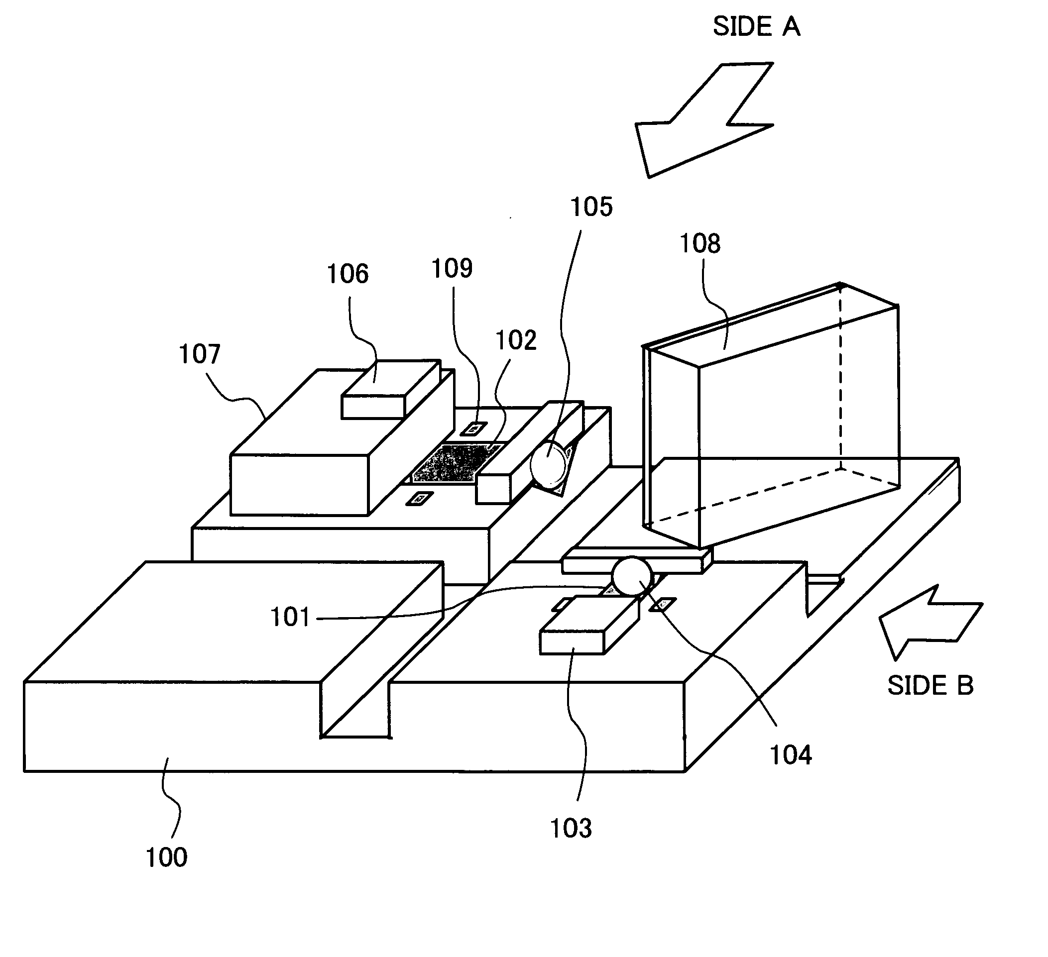
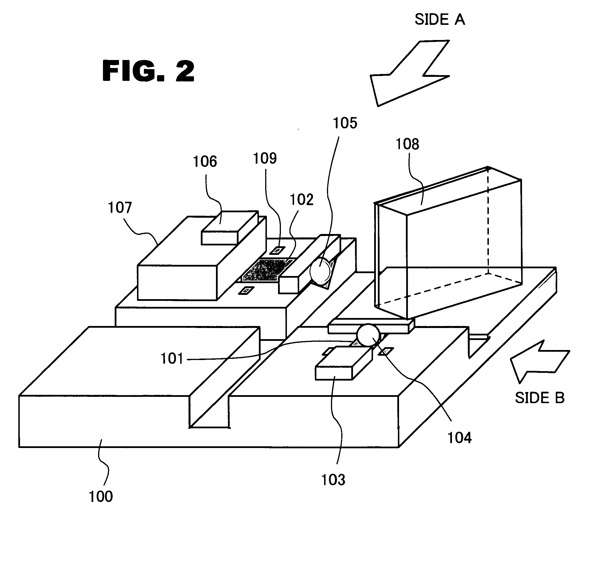
[0077]FIG. 2 illustrates a structure of a single core two-way optical communication module, to which the present invention can be applied. In a module shown in FIG. 2, an optical transmission unit (103), an optical receiving unit (106...


PUM


Abstract

A purpose of the present invention is to provide a micro-lens enabling in a simple and highly accurate manner to assess an amount of misalignment with an optical axis generated by an error in a process of manufacturing a micro-lens.
According to the present invention, the micro-lens manufactured using a semiconductor lens is provided with a lens portion, a peripheral portion located outside the lens portion and a mark for assessment formed near the peripheral portion during a process of manufacturing the lens portion.

Description

CROSS REFERENCE TO RELATED APPLICATION[0001]This application claims the priority of Application No. 2007-165700, filed Jun. 23, 2007 in Japan, the subject matter of which is incorporated herein by reference.TECHNICAL FIELD OF THE INVENTION[0002]The present invention relates to a micro-lens manufactured using a semiconductor substrate (silicon wafer). In particular, the present invention relates to a method of assessing to determine an error in an external shape in a manufacturing process of the micro-lens.BACKGROUND OF THE INVENTION[0003]Optical communication using an optical fiber represented by Fiber To The Home (FTTH) has become widely used. So called an “optical module” configured by aligning a laser as a light source and an optical fiber or an optical fiber and an optical receiver with high accuracy has been proposed.[0004]Patent Document 1 (Japan Patent Publication Number 3696802) disclosed a technology to manufacture a micro-lens with a size in an order of a few hundred micro...

Claims


Application Information

Patent Timeline
Patent Type & Authority Applications(United States)
IPC IPC(8): G02B13/00H01L23/544
CPCB29D11/00365H01L23/544H01L2223/54493H01L2924/0002H01L2924/00
Inventor SASAKI, HIRONORI
Owner LAPIS SEMICON CO LTD
Why Eureka
Try Eureka