
Eureka
For R&D, Eureka makes reading and utilizing patents & technical documents easy.
Eureka AIR
Designed for self-driven R&D workflows. Generate viable solutions, solve complex R&D challenges, empower your innovation with AI.

Eureka Materials
Designed for material experts only. Revolutionize your material R&D, from search, analyze, to developing new materials.

TechResearch
Generate reliable direction feasibility study reports for your R&D in just a few steps.

TechSeek
Discover and master advanced knowledge NOW. Basics, ideas, possibilities, all at once.

TechMind
As an expert in R&D Theories, TechMind can generates customized viable solutions instantly.

TechRisk
Analyze your overall solution with one click, know your potential R&D risks in advance.

TechMonitor
Get weekly tech updates, stay abreast of the latest tech innovations and key insights.
Two step chemical mechanical polish
- Summary
- Abstract
- Description
- Claims
- Application Information
AI Technical Summary
Benefits of technology
Problems solved by technology
Method used
Image

Examples
Embodiment Construction
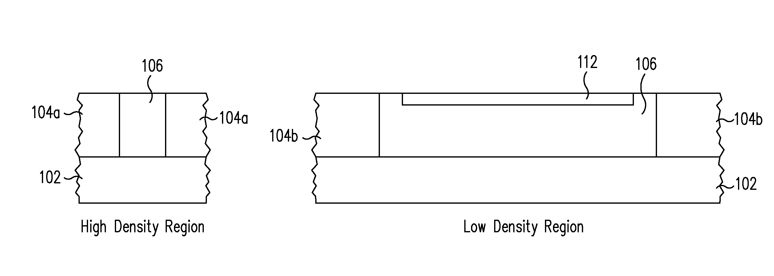
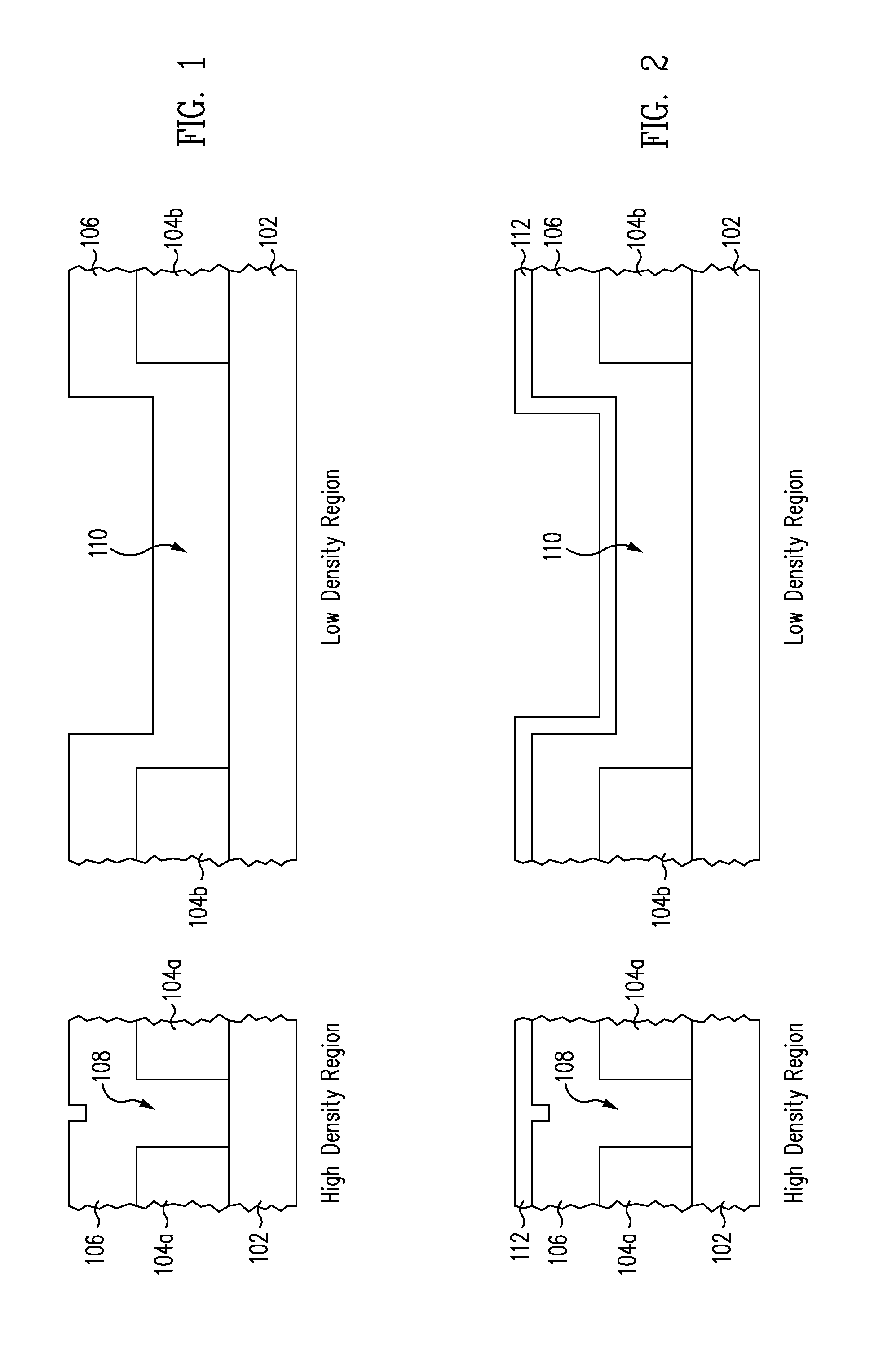
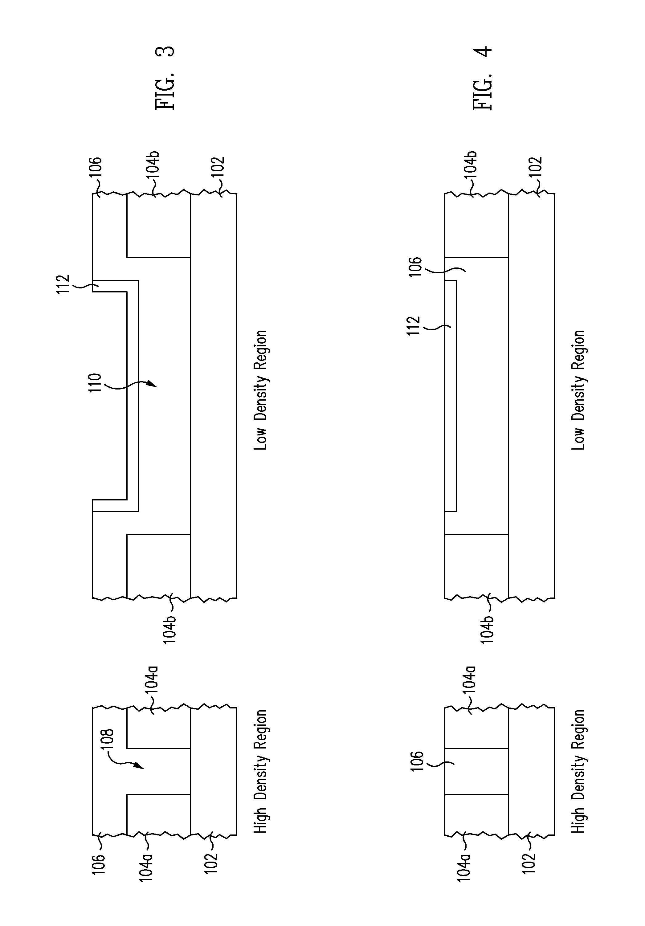
[0015]The present invention provides a method for two step chemical-mechanical planarization or polishing (CMP) that advantageously avoids dishing effects. FIGS. 1-4 illustrate cross-sectional views of one example of a semiconductor manufacturing process in which the present invention may be used.
[0016]Referring to FIG. 1, a cross-sectional view of a semiconductor substrate 102 with a high density pattern region and a low density pattern region is illustrated. Substrate 102 may be a wafer formed from a single crystalline silicon material, but may also comprise other materials, for example, an epitaxial material, a polycrystalline semiconductor material, or other suitable material. Substrate 102 may be doped by conventional means with dopants at different dosage and energy levels. It is noted that substrate 102 can further include additional layers, structures, and / or devices.
[0017]Structures 104a and 104b with a spacing therebetween are formed over substrate 102. In one example, str...
PUM
 Abstract
Description
Claims
Application Information
 - R&D Engineer
- R&D Manager
- IP Professional
- Industry Leading Data Capabilities
- Powerful AI technology
- Patent DNA Extraction
Browse by: Latest US Patents, China's latest patents, Technical Efficacy Thesaurus, Application Domain, Technology Topic, Popular Technical Reports.
© 2024 PatSnap. All rights reserved.Legal|Privacy policy|Modern Slavery Act Transparency Statement|Sitemap|About US| Contact US: help@patsnap.com