Method and System for Cooling a Bake Plate in a Track Lithography Tool

a technology of track lithography and bake plate, which is applied in the field of method and system for cooling bake plate of semiconductor processing tool, can solve the problems of lowering process chamber throughput, affecting process variability and ultimately device performance, and semiconductor fabrication process, so as to reduce the time used to cool, increase the throughput of the process chamber, and reduce the effect of tim

Inactive Publication Date: 2009-01-01
SOKUDO CO LTD
View PDF12 Cites 25 Cited by
  • Summary
  • Abstract
  • Description
  • Claims
  • Application Information

AI Technical Summary

Benefits of technology

[0013]Many benefits are achieved by way of the present invention over conventional techniques. For example, embodiments of the present invention reduce the time utilized to cool a bake plate, thereby increasing process chamber throughput. Additionally, embodiments of the present invention provide for uniform heat removal rates across the surface of the bake plate, thereby reducing the time used to bring the bake plate to a uniform temperature distribution at the new set point temperature. Depending upon the embodiment, one or more of these benefits, as well as other benefits, may be achieved. These and other benefits will be described in more detail throughout the present specification and more particularly below in conjunction with the following drawings.

Problems solved by technology

Lithography type device fabrication processes can be especially sensitive to variations in process recipe variables and the timing between recipe steps, which can directly affect process variability and ultimately device performance.
A drawback of this approach is that this cooling process is time-consuming, thereby lowering process chamber throughput.
Although this method generally provides more rapid cooling than convective air cooling, this method results in the generation of particles, which may lead to the formation of defects during the semiconductor fabrication process.

Method used


Image

  • Method and System for Cooling a Bake Plate in a Track Lithography Tool
  • Method and System for Cooling a Bake Plate in a Track Lithography Tool
  • Method and System for Cooling a Bake Plate in a Track Lithography Tool

Examples


Embodiment Construction

[0023]According to the present invention, techniques related to the field of substrate processing equipment are provided. More particularly, the present invention relates to a method and system for cooling a bake plate of a semiconductor processing apparatus. Merely by way of example, the method and system of the present invention utilize a cooling fluid to cool a bake plate in a bake chamber of a track lithography tool. The method and system can be applied to other characterization devices for semiconductor processing equipment utilized in other processing chambers. Embodiments of the present invention are described more fully below with reference to the accompanying drawings, where like numbers refer to like elements throughout.

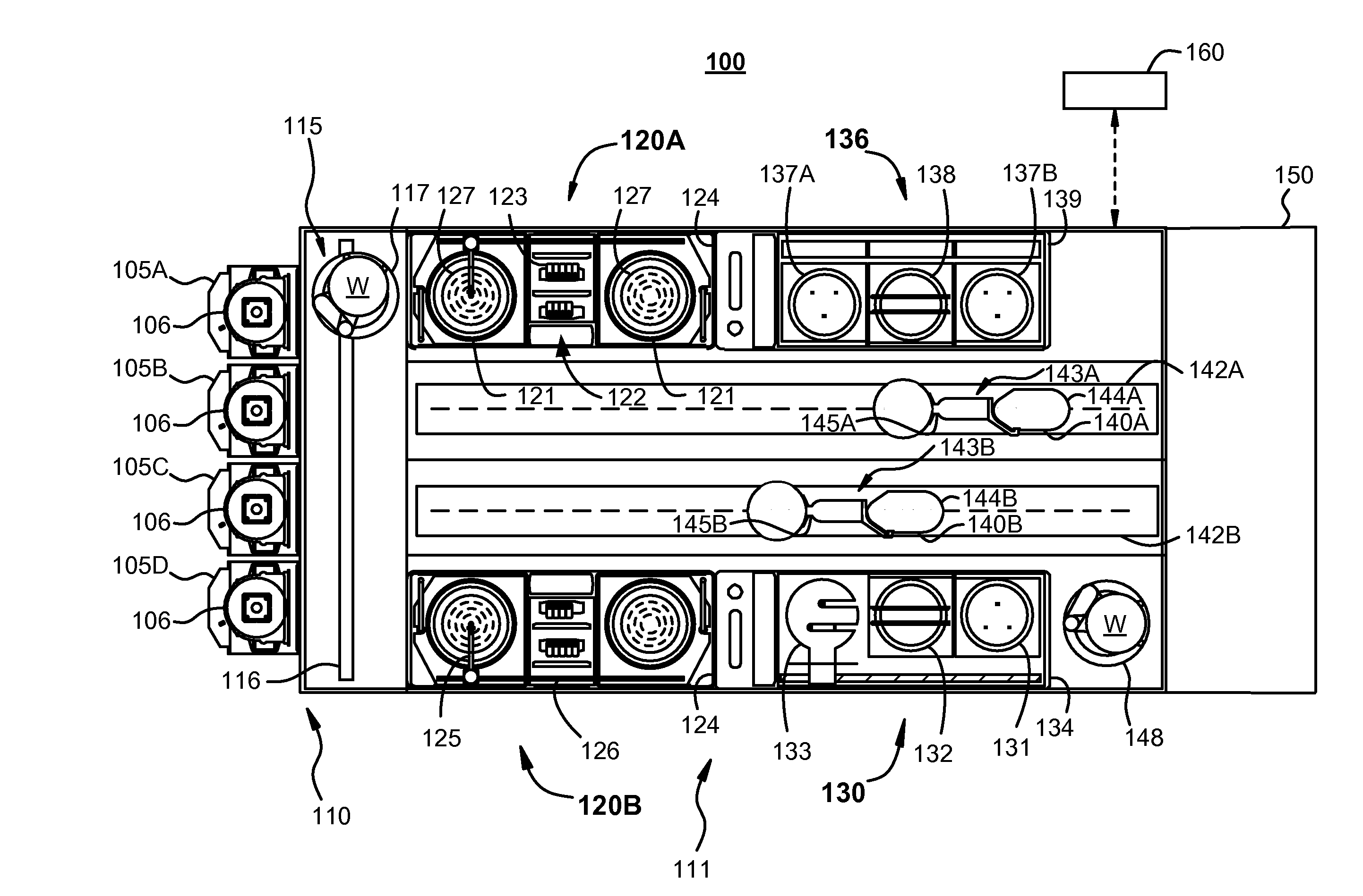
[0024]FIG. 1 is a simplified plan view of one configuration of a track lithography tool in which the embodiments of the present invention may be used. As illustrated in FIG. 1, the track lithography tool contains a front end module 110 (sometimes referred t...


PUM


Abstract

A bake station includes a bake plate having a thickness defined by a distance between an upper surface and a lower surface of the bake plate. The bake plate is configured to heat a substrate positioned adjacent the upper surface of the bake plate. The bake station also includes a base plate having a first surface positioned below and opposing the lower surface of the bake plate and a side plate extending between the lower surface of the bake plate and the first surface of the base plate. The side plate, the lower surface of the bake plate, and the first surface of the base plate define a space. The bake station further includes a plurality of nozzles coupled to the base plate. Each of the plurality of nozzles has an inlet configured to receive an input flow of fluid and an exit port configured to expel an exit flow of fluid onto the lower surface of the bake plate. Additionally, the bake station includes an exhaust port in fluid communication with the space and configured to exhaust the exit flow of fluid from the space.

Description

BACKGROUND OF THE INVENTION[0001]The present invention relates generally to the field of substrate processing equipment. More particularly, the present invention relates to a method and system for cooling a bake plate of a semiconductor processing tool. Merely by way of example, the method and system of the present invention utilize a cooling fluid to cool a bake plate in a bake chamber of a track lithography tool. The method and system can be applied to other characterization devices for semiconductor processing equipment utilized in other processing chambers.[0002]Modern integrated circuits contain millions of individual elements that are formed by patterning the materials that make up the integrated circuit, such as silicon, metal and / or dielectric layers, to sizes that are small fractions of a micrometer. One of the techniques used throughout the industry for forming such patterns is photolithography. A typical photolithography process sequence generally includes applying a unif...

Claims


Application Information

Patent Timeline
Patent Type & Authority Applications(United States)
IPC IPC(8): H05B3/68
CPCH01L21/67225H01L21/67109
Inventor KULKARNI, MAYUR G.
Owner SOKUDO CO LTD
Why Eureka
Try Eureka