Lightweight and compact through-silicon via stack package with excellent electrical connections and method for manufacturing the same
- Summary
- Abstract
- Description
- Claims
- Application Information
AI Technical Summary
Benefits of technology
Problems solved by technology
Method used
Image
Examples
Embodiment Construction
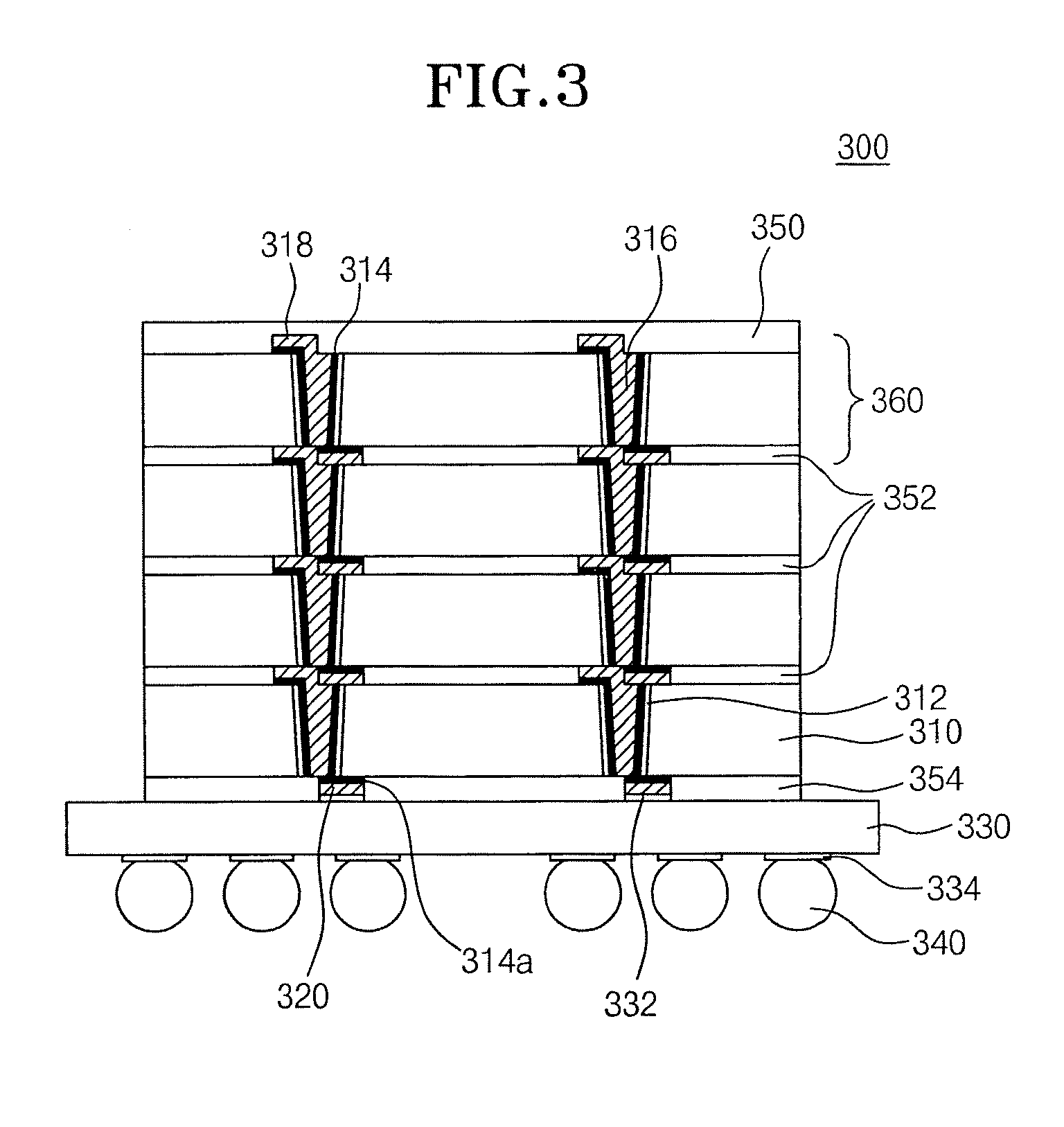
[0042]In the present invention, by forming through-silicon vias to have a small projecting height, it is possible to solve the problems of conventional stacked packages, which include: misalignment and increased height of a package resulting when a plurality of semiconductor chips are stacked.
[0043]In the present invention, in order to form a stack package, through-silicon vias are formed in each semiconductor chip. When the metal lines, which contact the upper and lower surfaces of the through silicon vias, are formed, one metal line is positioned on one half of the upper surface of each through-silicon via and another metal line positioned on the other half of the lower surface of each through-silicon via, with the metal line on the upper surface and the metal line on the lower surface facing opposite directions. Then at least two semiconductor chips having the structure just described above are stacked in a manner such that the metal line formed on one half of the upper surface o...
PUM
 Abstract
Description
Claims
Application Information


