Stack package that prevents warping and cracking of a wafer and semiconductor chip and method for manufacturing the same

Inactive Publication Date: 2009-01-01
SK HYNIX INC
View PDF5 Cites 64 Cited by
  • Summary
  • Abstract
  • Description
  • Claims
  • Application Information

AI Technical Summary

Benefits of technology

[0016]The embodiments of the present invention are directed to a stack package that prevents a wafer and semiconductor chip

Problems solved by technology

Therefore, when stacking the wafers or semiconductor chips having the through-silicon vias, the wafers or the semiconductor chips are likely to be warped due to a difference in thermal expansion coefficient, and it is

Method used


Image

  • Stack package that prevents warping and cracking of a wafer and semiconductor chip and method for manufacturing the same
  • Stack package that prevents warping and cracking of a wafer and semiconductor chip and method for manufacturing the same
  • Stack package that prevents warping and cracking of a wafer and semiconductor chip and method for manufacturing the same

Examples


Example

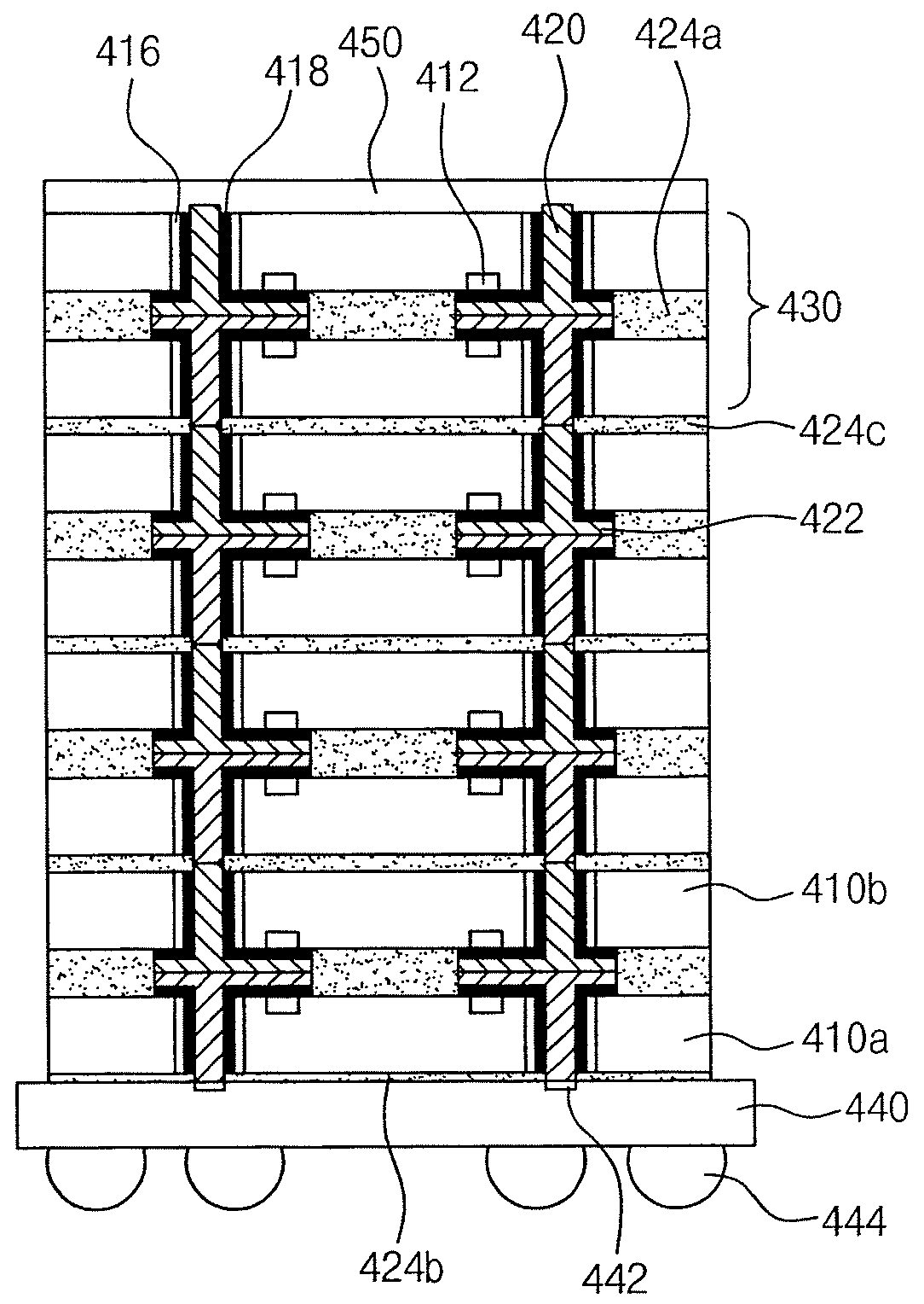
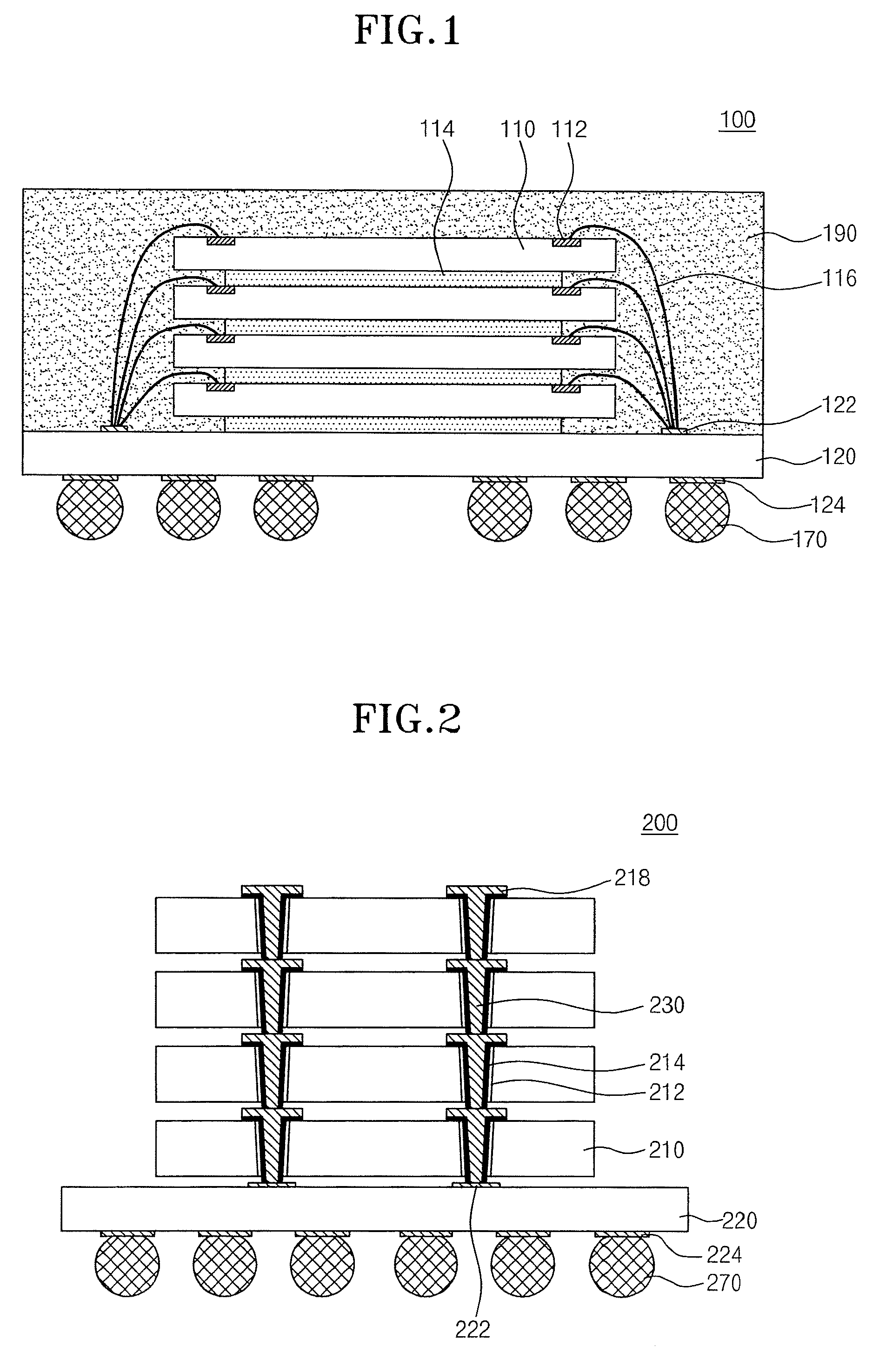
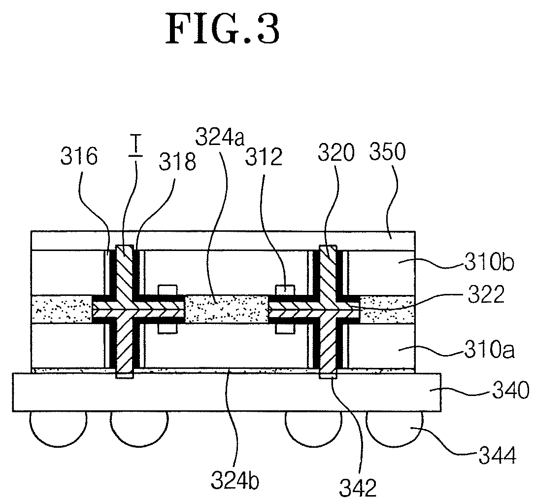
[0046]In the present invention, a method in which the lower surfaces of two wafers are back-grinded after stacking the wafers to be electrically connected is used, whereby a stack package using through-silicon vias is realized at a wafer level or a chip level. Also, in the present invention, the stack package is realized in a manner such that a single package unit or a plurality of package units is mounted to an external circuit having a substrate by the through-silicon vias. The through-silicon vias are exposed by back-grinding the lower surfaces of the respective stacked wafers. By doing this, the present invention solves the problems, which are caused by the decrease in thickness of the wafer and semiconductor chip, in the conventional art.

[0047]That is to say, in the present invention, first and second semiconductor chips, which are formed with through-silicon viasand redistribution layerredistribution layers that connect the through-silicon vias and bonding pads to each other, ...


PUM


Abstract

A stack package and a method for manufacturing the same. The stack package includes first and second semiconductor chips placed such that surfaces thereof, on which bonding pads are formed, face each other; a plurality of through-silicon vias formed in the first and second semiconductor chips; and a plurality of redistribution layers formed on the surfaces of the first and second semiconductor chips to connect the through-silicon vias to the corresponding bonding pad, wherein the redistribution layers of the first and second semiconductor chips contact each other. By forming the stack package in this manner, it is possible to prevent pick-up error and cracks from forming during the manufacturing process, and therefore the stack package can be reliable formed.

Description

CROSS-REFERENCE TO RELATED APPLICATIONS[0001]The present application claims priority to Korean patent application number 10-2007-0063181 filed on Jun. 26, 2007, which is incorporated herein by reference in its entirety.BACKGROUND OF THE INVENTION[0002]The present invention relates to a stack package and a method for manufacturing the same, and more particularly, to a stack package which prevents a wafer and semiconductor chips from being warped and also prevents cracks from occurring during a manufacturing process, and a method for manufacturing the same.[0003]The packaging technology for a semiconductor integrated circuit has been continuously evolving to meet the demands of miniaturization and high capacity. Recently, various techniques for stack packages have been disclosed in the art to provide satisfactory results in terms of miniaturization, high capacity, and mounting efficiency.[0004]The term “stack”, as referred to in the semiconductor industry, means to vertically pile at ...

Claims


Application Information

Patent Timeline
IPC IPC(8): H01L23/48H01L21/60
CPCH01L24/94H01L2924/014H01L2224/16H01L2224/48091H01L2225/06513H01L2225/06517H01L2225/06527H01L2225/06541H01L2924/01013H01L2924/01029H01L2924/01033H01L2924/01075H01L2924/01078H01L2924/01079H01L2924/01082H01L2924/14H01L2924/15311H01L25/0657H01L2924/01006H01L2924/01005H01L2924/00014H01L2924/181H01L2224/05001H01L2224/05611H01L2224/05624H01L2224/05644H01L2224/05655H01L2224/32145H01L2224/73265H01L21/76898H01L24/08H01L2224/08145H01L2224/08146H01L24/05H01L24/02H01L2924/0001H01L2224/02372H01L2224/05548H01L2924/00012H01L2224/02H01L23/12H01L2224/13025
Inventor CHUNG, QWAN HO
Owner SK HYNIX INC
Why Eureka
Try Eureka