Method and a system for optical design and an imaging device using an optical element with optical aberrations

a technology of optical aberration and design method, which is applied in the field of optical design and imaging device design, can solve the problems of imaging system, further blurring of image, and all imaging systems having a certain level of blurring

Inactive Publication Date: 2009-01-01
SAMSUNG ELECTRONICS CO LTD
View PDF5 Cites 22 Cited by
  • Summary
  • Abstract
  • Description
  • Claims
  • Application Information

AI Technical Summary

Benefits of technology

[0014]According to one aspect of the present invention there is provided an imaging apparatus for outputting a final image having a predefined mapping. The imaging apparatus comprises an image sensor, an optical unit having an optical aberration, which is designed for projecting a uncorrected initial image on the image sensor. The imaging apparatus further comprises an optical algorithmic correction module, operatively connected to the image sensor, which is designed for compensating for the effect of the optical aberration on the uncorrected initial image according to at least one parameter defined according to the optical aberration. In such a manner, the optical algorithmic correction allows the outputting the final image without the effect produced by the optical aberration and with the predefined mapping.
[0015]According to another aspect of the present invention there is provided an imaging apparatus for outputting a final image having a predefined mapping. The imaging apparatus comprises an image sensor, an optical unit having an image distortion aberration above 5%, configured for projecting an uncorrected initial image on the image sensor, and an optical algorithmic correction module that is operatively connected to the image sensor. The optical algorithmic correction module compensates for the effect of the optical aberration on the uncorrected initial image, thereby allowing the outputting the final image without the effect of the optical aberration and with the predefined mapping.
[0017]According to another aspect of the present invention there is provided an imaging apparatus for outputting a final image having a predefined mapping. The imaging apparatus comprises an image sensor, an optical unit having a chromatic optical aberration, configured for projecting a uncorrected initial image with a first area and a second area on the image sensor, the first and second areas having different resolutions, and an optical algorithmic correction module, operatively connected to the image sensor, configured for compensating for the effect of the optical aberration on the uncorrected initial image, thereby allowing the outputting the final image without the effect of the optical aberration and with the predefined mapping.
[0019]According to another aspect of the present invention there is provided a system for designing an imaging device. The system comprises an input module configured for receiving a specification of a final image mapping a three-dimensional environment according to a predefined mapping an optical unit having an optical aberration. The system further comprises an optical design module for providing an optical design of the optical unit having the optical aberration, the optical unit is configured for projecting a distorted initial image. The system further comprises an algorithmic correction module for generating an algorithmic correction for compensating for the effect of the optical aberration on the image, the algorithmic correction is defined according to the predefined mapping and the optical aberration. In addition, the system further comprises an output module for outputting the optical design and the algorithmic correction, thereby allowing the manufacturing of an imaging device configured for outputting the final image.

Problems solved by technology

However, due to diffraction, all imaging systems have a certain level of blurring.
Moreover, imaging systems also suffers from optical aberrations which further blur the image.
It should be noted that the optical aberrations not only reduce resolution but also cause uneven resolution across the field of view (FOV) of the display at one or more colors.
It should be noted that such a finalizing of the optical design does not necessarily achieve desired performance.

Method used


Image

  • Method and a system for optical design and an imaging device using an optical element with optical aberrations
  • Method and a system for optical design and an imaging device using an optical element with optical aberrations
  • Method and a system for optical design and an imaging device using an optical element with optical aberrations

Examples


Embodiment Construction

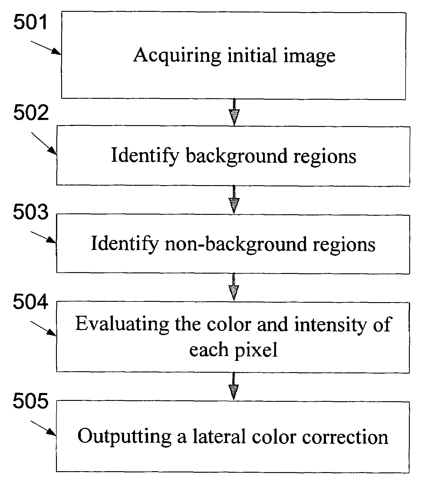
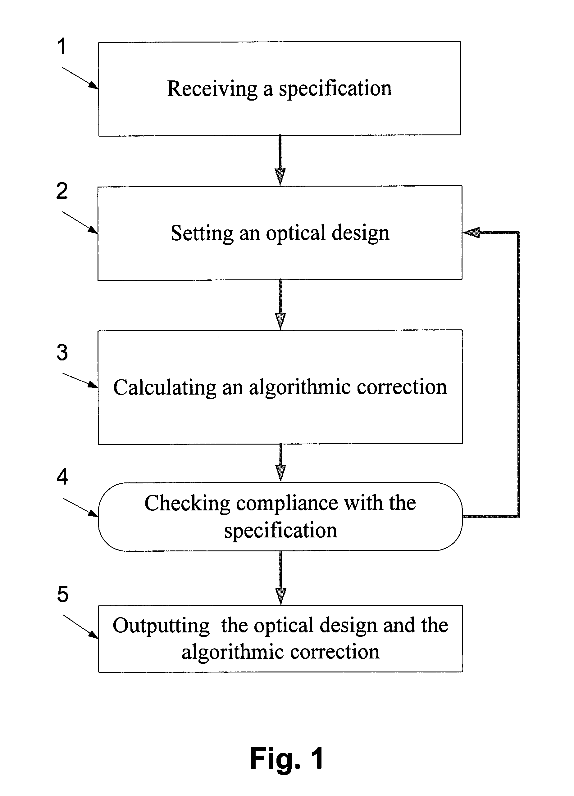
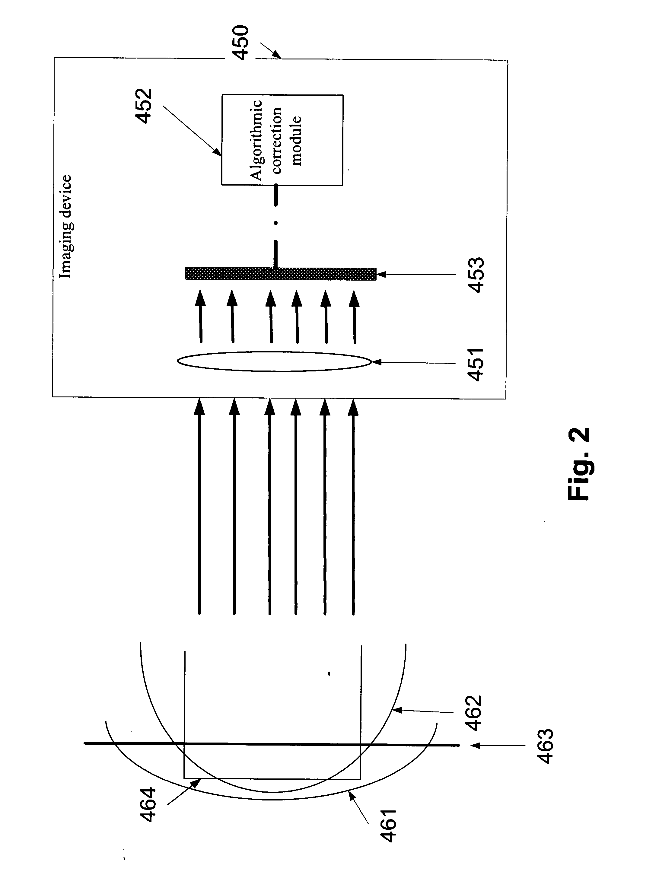
[0034]The present embodiments comprise a system and a method for designing an imaging device, such as a camera, with an optical unit, such as a lens assembly, with one or more optical aberrations, such as image distortion and lateral color, optionally predefined in the optical design stage.

[0035]The method comprises a number of steps. During the first step, a specification that defines a final image that maps a three-dimensional environment according to a predefined mapping is provided. The three-dimensional environment may include one or more objects. Light reflected from each object may have a different projection, as further described below. Additionally, the specification defines or an optic unit with one or more optical aberrations. The optical unit projects uncorrected initial image, which is hampered by the optical aberrations. The specification may regard to the characteristics of the image sensor which is used in the imaging device. After the specification has been received...


PUM


Abstract

A method for designing an imaging device. The method comprises receiving specification of a final image mapping a three-dimensional environment according to a predefined mapping and an optical unit with an optical aberration. The method further comprises estimating an optical design of the optical unit with the optical aberration. The optical unit is configured for projecting a uncorrected initial image according to the optical aberration. The method further comprises calculating an algorithmic correction for the uncorrected initial image. The algorithmic correction is designed for compensating for the effect of the optical aberration on the uncorrected initial image. The method further comprises manufacturing the imaging device. The manufactured imaging device having the optical design and applying the algorithmic correction on the uncorrected initial image, thereby outputting the final image without the effect produced by said optical aberration and with said predefined mapping.

Description

FIELD AND BACKGROUND OF THE INVENTION[0001]The present invention relates to a method and a system for a design of an imaging device and, more particularly, but not exclusively, to a method and a system for designing an optical unit and calculating a correction to one or more aberrations thereof.[0002]In recent years, the demand for high performance compact digital imaging devices has increased. Such imaging devices convert an image of an intercepted scene to electronic signals by using an image sensor, such as a charge-coupled device (CCD) based sensor or a complementary metal-oxide semiconductor (CMOS) based sensor. In particular, the demand for high performance compact digital imaging devices, which are designed to be mounted in a compact device, such as a mobile phone, and have image sensors that have large number of pixels, more than two million pixels, is increasing. Such a demand is and outcome of the prevalence of mobile devices that incorporate digital cameras, such as lapto...

Claims


Application Information

Patent Timeline
Patent Type & Authority Applications(United States)
IPC IPC(8): H04N5/74G02B5/00G03B13/18H04N5/238H04N5/335
CPCH04N5/217H04N9/045H04N5/3572G06T5/006H04N23/81H04N25/61H04N25/611H04N25/60
Inventor SOREK, NOAMSADE, SHARON
Owner SAMSUNG ELECTRONICS CO LTD
Why Eureka
Try Eureka