

Over-Voltage and Under Voltage Protection Circuit
- Summary
- Abstract
- Description
- Claims
- Application Information
AI Technical Summary
Benefits of technology
Problems solved by technology
Method used
Image

Examples
Embodiment Construction
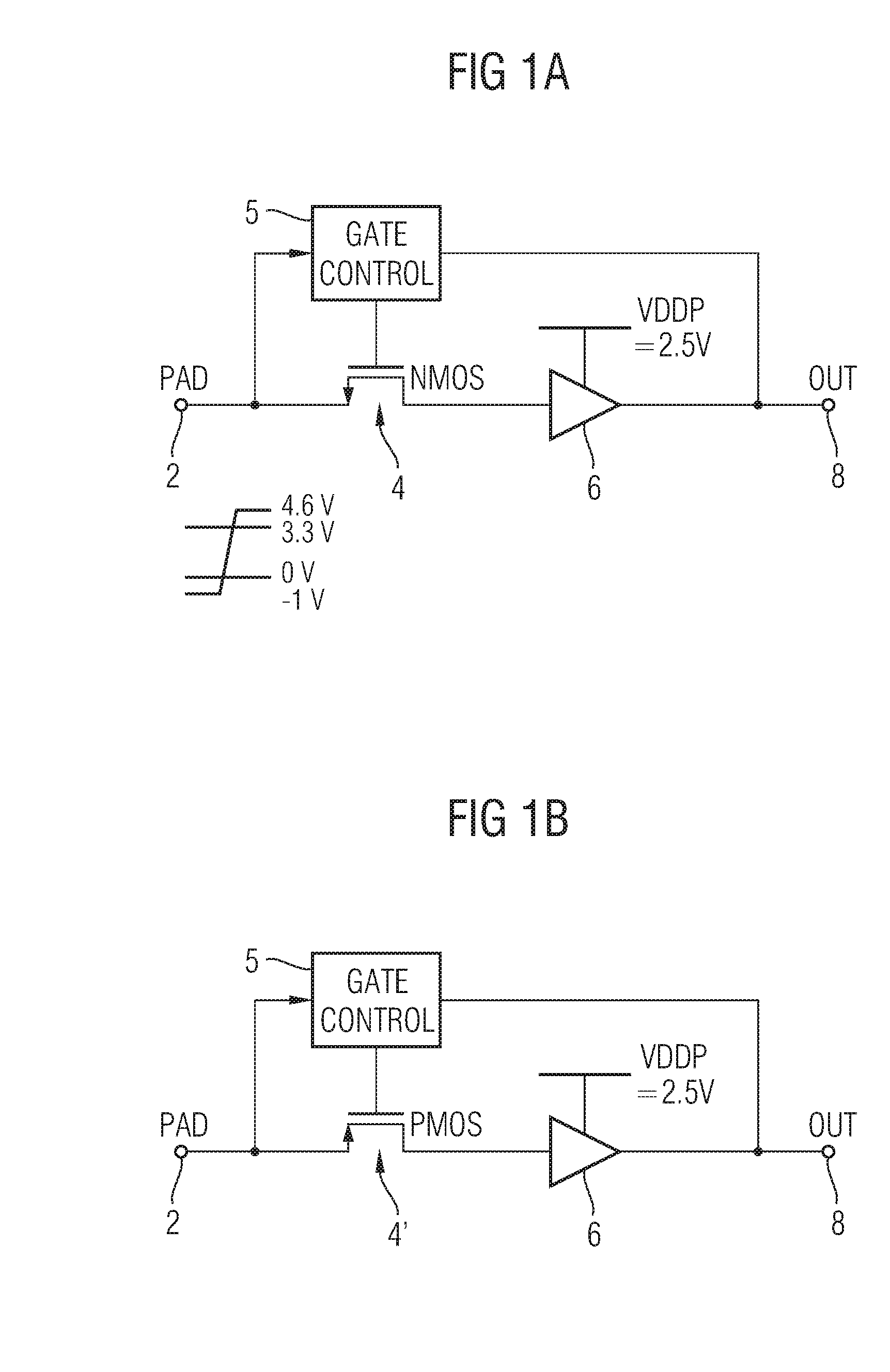
[0043]FIG. 1a shows a circuit diagram of a protection circuit according to a first embodiment of the invention. FIG. 1b shows a circuit diagram of a protection circuit according to a second embodiment of the invention. FIGS. 1a and 1b illustrate the basic principles behind the invention.
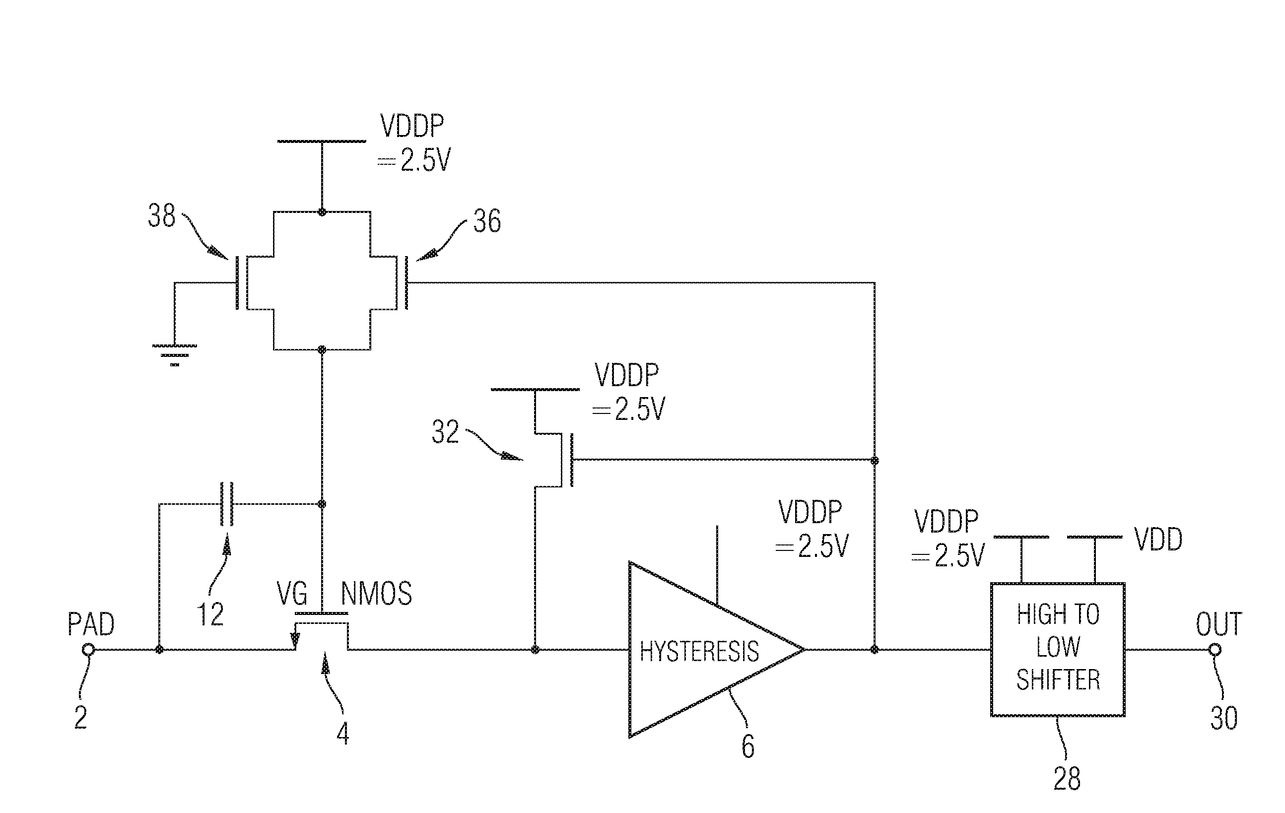
[0044]Referring to FIG. 1a, an incoming signal is applied to a pad 2 which is connected to the source of a pass transistor 4 (which is an NMOS transistor) and also to one input of a gate control circuit 5. The gate of the pass transistor 4 is connected to the output of the gate control circuit 5 and the drain of the pass transistor 4 is connected to the input of a hysteresis inverting stage 6. The output of the hysteresis stage 6 is connected to a further input to the gate control circuit 5 and also to an output 8 of the circuit.
[0045]The present invention is of particular applicability to a Universal Serial Bus (USB) receiver circuit. The normal signaling level for a USB is 0 to 3.3 V. However, the ...
PUM
 Abstract
Description
Claims
Application Information