
Block addressing for parallel memory arrays

Inactive Publication Date: 2009-01-08
MICRON TECH INC
View PDF26 Cites 43 Cited by
  • Summary
  • Abstract
  • Description
  • Claims
  • Application Information

AI Technical Summary

Problems solved by technology

For example, a memory cell can fail for being stuck in a particular logic state, for not meeting a timing specification, or the like.
Cells can also fail in the field.
For example, many non-volatile memory types can wear out over multiple write cycles.
Bad or unusable memory cells can affect the usability of higher order memory units.
For example, bad cells can cause a row to be unusable, and the page(s) of the row to be unusable.
When an insufficient number of pages for a block is available, the entire block may be marked as a bad block, and none of the pages of that block are typically accessible.
A problem arises in the handling of bad blocks.
However, if the addresses are not sequential, then the preloading may not occur efficiently.
For example, the technique illustrated in FIG. 3 typically uses some form of internal controller intervention to select the replacement block(s) and to combine data from separate internal memory reads, which further slows down access.
However, the third block 3A 410 from array A 402 is not paired with the third block 3B 418 from array B 404 because the third block 3B 418 is bad and is not usable.
However, the third block 3A 410 is not utilized despite its viability and is effectively treated as a bad block.
This decreases the number of available blocks for an array, and if the effective number of good blocks falls below the minimum specified, this can decrease the production yield and increase the cost of production.

Method used


Image

  • Block addressing for parallel memory arrays
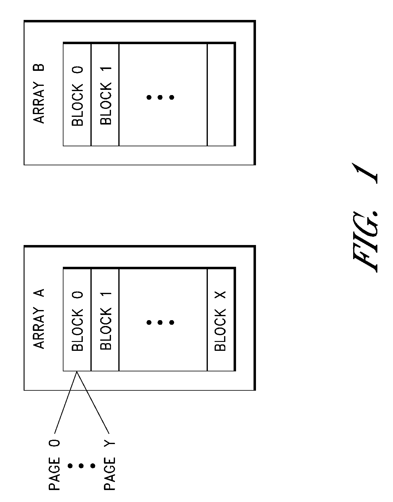
  • Block addressing for parallel memory arrays
  • Block addressing for parallel memory arrays

Examples


Embodiment Construction

[0031]Although particular embodiments are described herein, other embodiments of the invention, including embodiments that do not provide all of the benefits and features set forth herein, will be apparent to those of ordinary skill in the art.

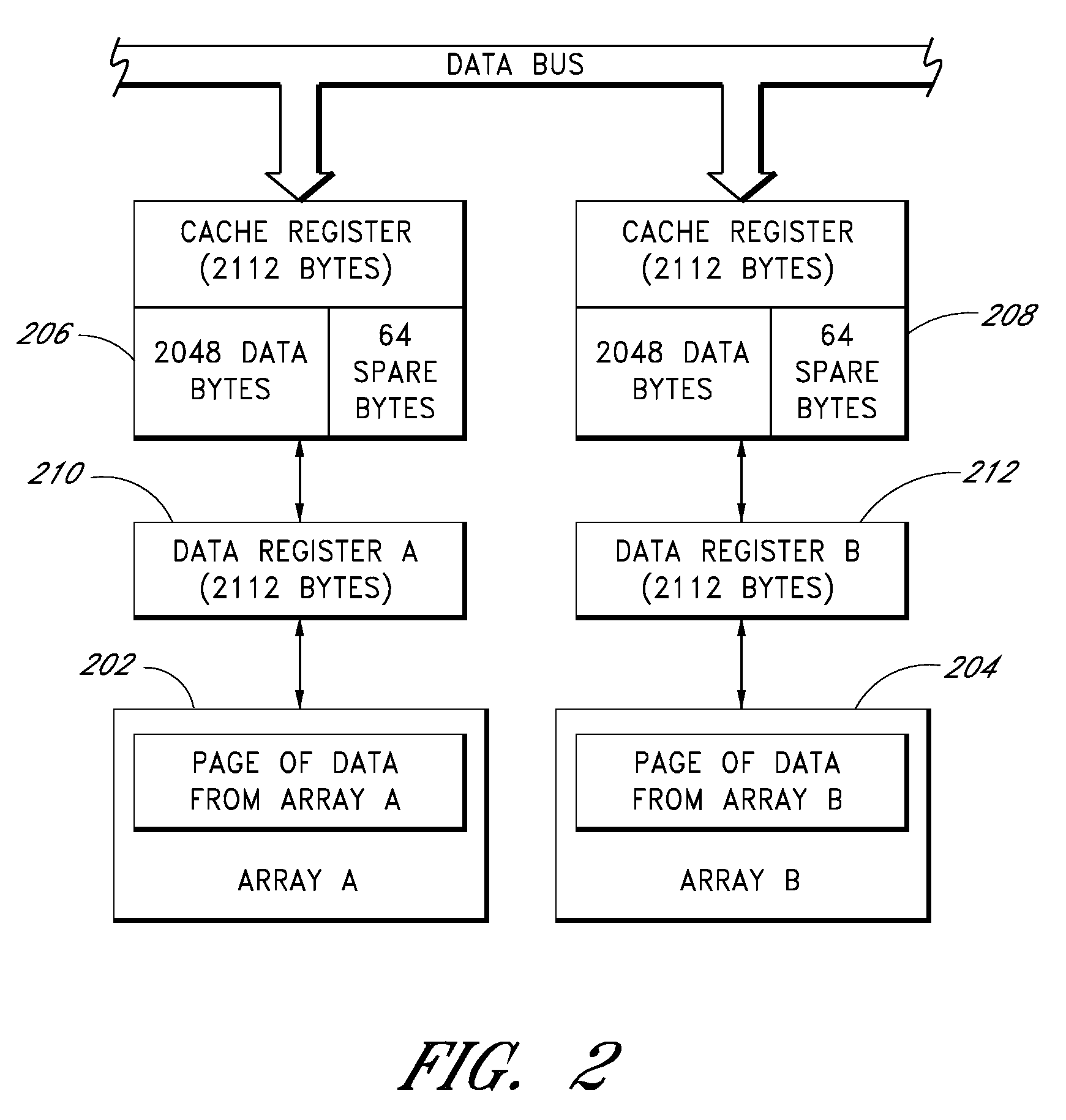
[0032]One embodiment of the invention provides associative mapping of the blocks of two or more memory arrays such that data, such as pages of data, from good blocks of the two or more memory arrays can be written or read in an alternating manner for speed or can be written to read in parallel for providing data to relatively wide data channels. For example, this obviates controller intervention to access associated data spread among disparate rows and can increase the throughput of data by providing, where configured, the ability to alternate reading of data from two or more arrays. For example, while data from one array is being loaded to a cache, data from another array that has already been loaded to the cache can be read. In one example, ...


PUM


Abstract

Apparatus and methods provide associative mapping of the blocks of two or more memory arrays such that data, such as pages of data, from the good blocks of the two or more memory arrays can be read in an alternating manner for speed or can be read in parallel for providing data to relatively wide data channels. This obviates the need for processor intervention to access data and can increase the throughput of data by providing, where configured, the ability to alternate reading of data from two or more arrays. For example, while one array is loading data to a cache, the memory device can be providing data that has already been loaded to the cache.

Description

BACKGROUND[0001]1. Field of the Invention[0002]Embodiments of the invention generally relate to integrated circuits. In particular, embodiments of the invention relate to memory circuits.[0003]2. Description of the Related Art[0004]Semiconductor memory devices are ubiquitous in digital electronics devices. Examples of these devices include computers, cameras, digital media players, games, personal digital assistants, mobile phones, navigation devices, non-volatile storage products, and the like. Examples of non-volatile storage products include CompactFlash (CF) cards, MultiMedia cards (MMC), secure digital (SD) cards, Flash PC cards (e.g., ATA Flash cards), SmartMedia cards, solid-state disks (SSDs), hybrid hard drives, and memory sticks. Semiconductor memory provides storage and retrieval of data.[0005]There exist many types of semiconductor memories. Examples of memories include various types of random access memory (RAM) (including SRAM, DRAM, and SDRAM), flash memory, electrica...

Claims


Application Information

Patent Timeline
IPC IPC(8): G06F12/06
CPCG06F12/0246G06F12/0292G11C29/76G06F2212/7208G11C8/12G06F2212/7201G06F3/0611G06F3/0619G06F3/064G06F3/0656G06F3/0688G06F12/0853G06F12/1072G06F2212/1024G06F2212/2022G06F2212/283
Inventor EGGLESTON, DAVID
Owner MICRON TECH INC
Learn More