Variable work function transistor high density mask ROM

a work function transistor and mask rom technology, applied in the field of information storage, can solve the problems of difficult to increase the cell density using this programming technique, difficult to further reduce the size of field effect transistors used, and difficulty in increasing storage density

Inactive Publication Date: 2002-07-09
UNITED MICROELECTRONICS CORP
View PDF4 Cites 24 Cited by
  • Summary
  • Abstract
  • Description
  • Claims
  • Application Information

AI Technical Summary

Problems solved by technology

Difficulties are encountered when attempting to increase the storage density of mask ROMs following conventional strategies.
Difficulties encountered in achieving precise alignment in a production environment makes it difficult to further reduce the size of the field effect transistors used in forming the mask ROM while still obtaining acceptable yields.
In addition, it is difficult to form sufficiently thick insulating films for small cell sizes, so that it is difficult to increase the cell density using this programming technique.
As such, it is increasingly difficult to implement this programming technique for smaller design rules.
Several problems can occur in the conventional implantation programming technique which preclude this technology from being scaled down for use in smaller design rules.
Diffusion from the implant regions parallel to the bit lines limits how closely word lines can be spaced, which in turn limits the extent to which the ROM cell can be miniaturized.
Other difficulties with the implantation programming technique arise from possible misalignment of the programming mask.
If the adjacent region represents a memory location for which implantation should be made, then this misalignment can generate an error, particularly when the misalignment is coupled with the subsequent diffusion of impurities.
Implantations into the channel region are not self-aligned to the buried N.sup.+ lines so that misalignment of the edge of the mask opening defining the implantation along the word line direction is a possible source of error.

Method used


Image

  • Variable work function transistor high density mask ROM
  • Variable work function transistor high density mask ROM
  • Variable work function transistor high density mask ROM

Examples


Embodiment Construction

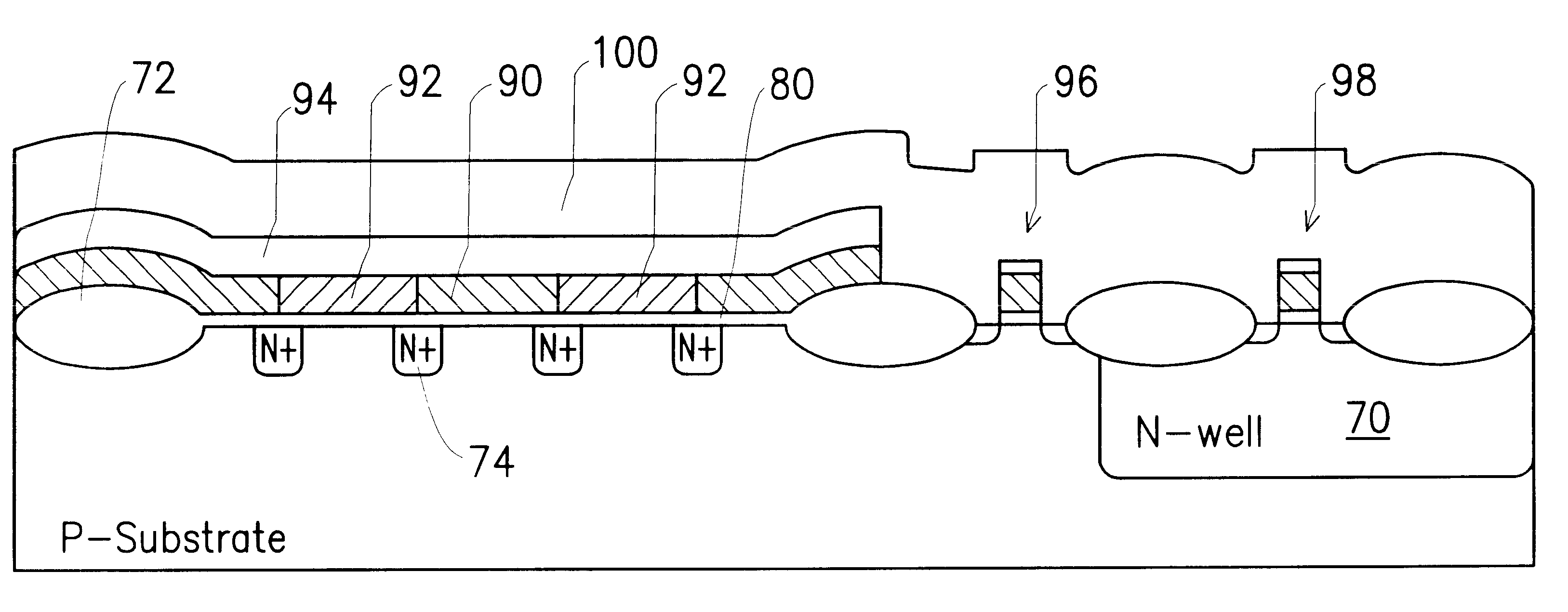
One aspect of the present invention provides a memory device comprising a first transistor having a drain, a source and a gate and a second transistor having a drain, a source and a gate. The first and second transistors have a common drain, a common source, or both a common drain and a common source. The gate of the first transistor comprises polysilicon doped P-type and the gate of the second transistor comprises polysilicon doped N-type. In accordance with a further aspect of the present invention, the gates of the first and second transistor consist of a lower polysilicon layer and a second layer of a conductive material which makes ohmic contact to N-type polysilicon and P-type polysilicon.

Another embodiment of the present invention memory device comprises a first transistor and a second transistor. The gate of the first transistor comprises a lower polysilicon layer doped N-type and an upper layer of conductive material, the upper layer of conductive material forming an ohmic ...


PUM


Abstract

A mask ROM stores information by selecting the work function of the gates of each FET in an array of FETs. The polysilicon gates of some of the FETs are doped N-type and the gates of the other FETs are doped P-type to form gates having different work functions, thereby forming FETs having different threshold voltages. The ROM consists of a parallel array of buried N+ bit lines formed in the substrate, a gate oxide layer deposited over the bit lines and a layer of polysilicon deposited on the gate oxide. The polysilicon is blanket doped P-type and then an encoding mask is formed, with openings in the encoding mask exposing regions of the polysilicon to be formed into gates of FETs with low threshold voltages. Either arsenic or phosphorus is doped into the polysilicon through the mask openings. The mask is removed, a layer of conductive material such as tungsten silicide is deposited and the polysilicon and the conductive material are formed into word lines for the ROM. The word lines of the ROM serve as gates for the FETs and the bit lines serve as sources and drains for the FETs.

Description

1. Field of the InventionThe present invention relates to the storage of information by altering the operational characteristics of a transistor within an array of memory transistors and, more particularly, to a read only memory (ROM).2. Description of the Related ArtDifficulties are encountered when attempting to increase the storage density of mask ROMs following conventional strategies. Alignment during mask ROM programming is important to the proper storage of information within mask ROMS. Difficulties encountered in achieving precise alignment in a production environment makes it difficult to further reduce the size of the field effect transistors used in forming the mask ROM while still obtaining acceptable yields. Certain of the difficulties in reducing the size of mask ROMs are discussed as follows.A portion of a mask ROM 10 is schematically illustrated in FIG. 1 as including a parallel array of word lines WL and a parallel array of bit lines BL. Programming of the ROM 10 is...

Claims


Application Information

Patent Timeline
Patent Type & Authority Patents(United States)
IPC IPC(8): H01L21/70H01L21/8246H01L21/8239H01L27/112
CPCH01L27/112H01L27/11233H01L27/1052H10B99/00H10B20/00H10B20/36
Inventor SHEU, SHING-RENKUNG, CHENG-CHIH
Owner UNITED MICROELECTRONICS CORP
Why Eureka
Try Eureka