Method of creating mask layout image and imaging system

a mask layout and image technology, applied in the field of semiconductor devices, can solve the problems of raising lithography costs and lithography costs, and achieve the effects of reducing the value of an image fitting function, high contrast, and high fidelity

Inactive Publication Date: 2009-01-08
SAMSUNG ELECTRONICS CO LTD
View PDF4 Cites 9 Cited by
  • Summary
  • Abstract
  • Description
  • Claims
  • Application Information

AI Technical Summary

Benefits of technology

[0011]According to embodiments of the present invention, by using a weighting function having a none-zero value with a predetermined critical range and a convolution kernel, a mask layout pattern with high contrast and high fidelity can be obtained. The critical range may be determined in consideration of various tones of a mask field and, therefore, a mask layout pattern may be easily formed regardless of the tones of the mask field.
[0012]According to another aspect of the present invention, there is provided an imaging sys...

Problems solved by technology

As a result, the size of a pattern transcribed on a wafer becomes actually smaller than the wavelength of an exposure beam and thus an optical proximity effect caused by diffraction and interference of the exposure beam becomes a critical factor that determines limitation of resolution.
However, the assist ...

Method used


Image

  • Method of creating mask layout image and imaging system
  • Method of creating mask layout image and imaging system
  • Method of creating mask layout image and imaging system

Examples


Embodiment Construction

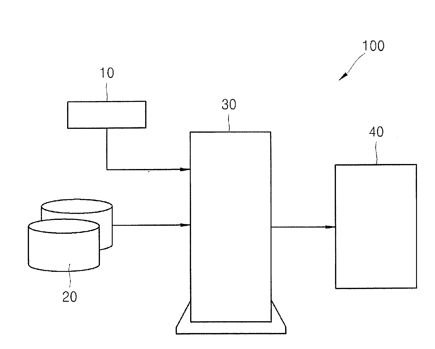
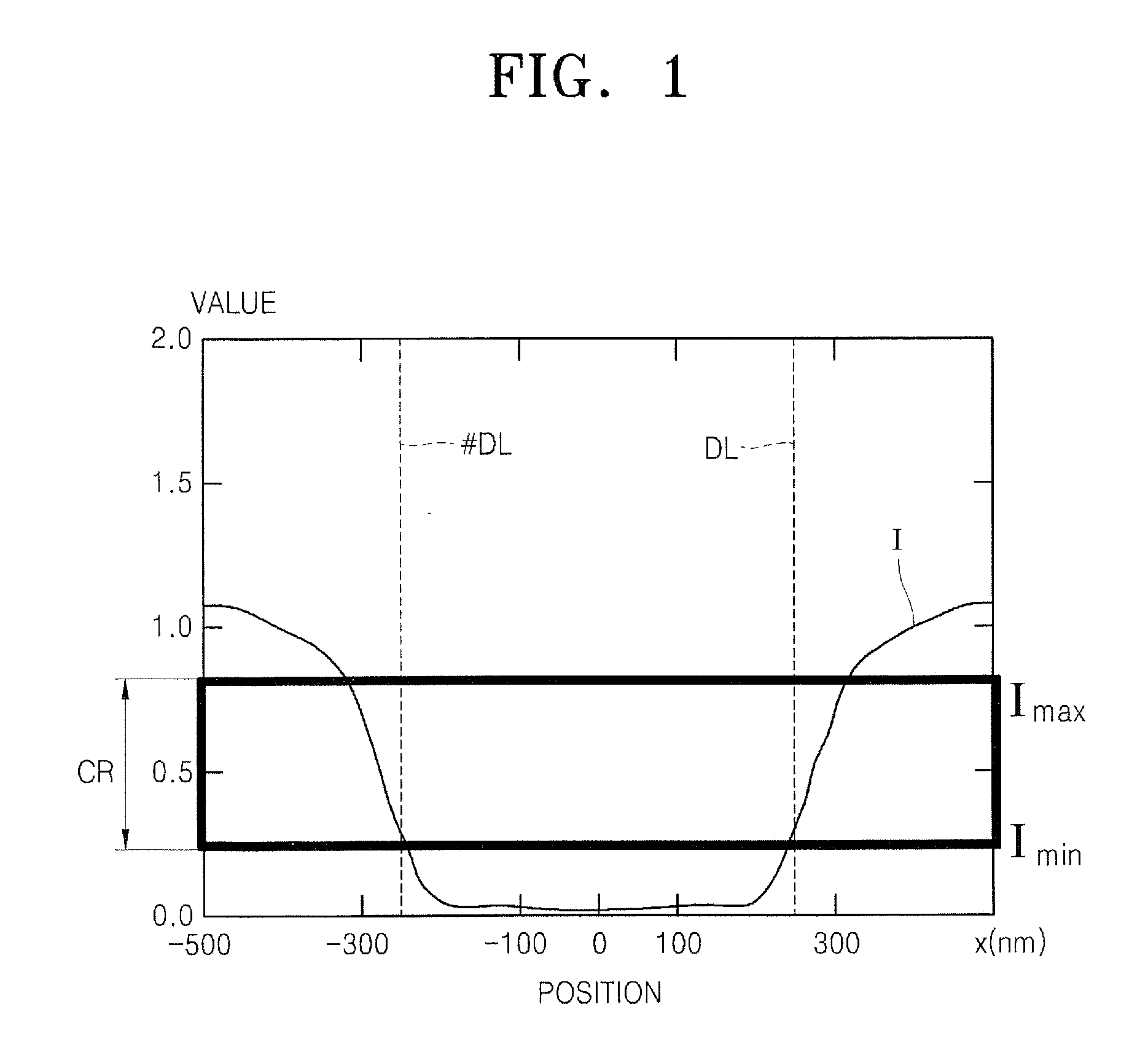
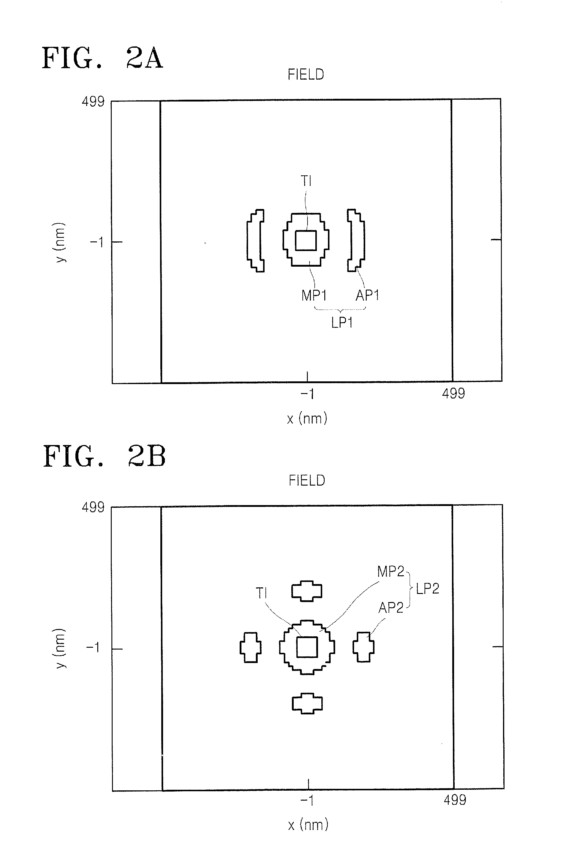
[0017]Hereinafter, the present invention will be described in detail by explaining embodiments of the invention with reference to the attached drawings.

[0018]The invention may, however, be embodied in many different forms and should not be construed as being limited to the embodiments set forth herein; rather, these embodiments are provided so that this disclosure will be thorough and complete, and will fully convey the concept of the invention to those of ordinary skill in the art.

[0019]It will also be understood that when a layer is referred to as being “on” another layer or substrate, it can be directly on the other layer or substrate, or intervening layers may also be present. In the drawings, the thicknesses of layers and regions are exaggerated for clarity. Like reference numerals in the drawings denote like elements. As used herein, the term “and / or” refers to one of or a combination of at least two of listed items.

[0020]The terminology used herein is for the purpose of descr...


PUM


Abstract

Provided are a method of creating a mask layout image from a target image, a computer readable storage medium having stored thereon a computer program for executing the method, and an imaging system. The method includes reading all or a part of a target image to be transcribed on a substrate; defining a mask data set including a plurality of pixels having a predetermined transmittance characteristic; defining a weighting function having a non-zero value within a critical range; defining a convolution kernel determined by an illumination meter; and creating the mask layout image that minimizes an image fitting function by using the weighting function and the convolution kernel.

Description

CROSS-REFERENCE TO RELATED PATENT APPLICATION[0001]This application claims the benefit of Korean Patent Application No. 10-2007-0067748, filed on Jul. 5, 2007, in the Korean Intellectual Property Office, the disclosure of which is incorporated herein in its entirety by reference.BACKGROUND OF THE INVENTION[0002]The present invention relates generally to semiconductor devices, and more particularly, to systems and methods for manufacturing semiconductor devices.[0003]Due to development of photolithography technology, scale reduction of large scale integrated circuits (LSIs) has been accelerated. Currently, design rules for manufacturing semiconductor devices are continuously reduced and scale reduction reaches 90 nm, 65 nm, 45 nm, and even a smaller size than 45 nm. As a result, the size of a pattern transcribed on a wafer becomes actually smaller than the wavelength of an exposure beam and thus an optical proximity effect caused by diffraction and interference of the exposure beam b...

Claims


Application Information

Patent Timeline
IPC IPC(8): G06F17/50
CPCG03F1/144G03F7/705G03F1/36G03F1/70
Inventor HWANG, CHANCHO, HAN-KULEE, SUK-JOO
Owner SAMSUNG ELECTRONICS CO LTD
Why Eureka
Try Eureka