Chip-type LED and method of manufacturing the same

a chip-type led and manufacturing method technology, applied in the manufacture of printed circuits, printed circuit aspects, solid-state devices, etc., can solve the problems of low upward reflective efficiency, increased cost of chip-type leds, and difficulty in achieving slim size, so as to reduce manufacturing costs, reduce the height of metallic small-gauge wires, and facilitate the manufacturing method

Active Publication Date: 2009-01-15
SHARP KK
View PDF10 Cites 36 Cited by
  • Summary
  • Abstract
  • Description
  • Claims
  • Application Information

AI Technical Summary

Benefits of technology

[0020]According to the manufacturing method of the present invention, forming a wiring pattern or the like around the outside of the insulating substrate is not necessary, which makes the manufacturing method that much easier, and can also reduce the manufacturing cost. In addition, when laser light is irradiated onto the portion of the insulating substrate at which the LED chip is to be mounted, and a through-hole is formed so as to reach the metallic sheet on the rear surface of the insulating substrate, the laser light removes the insulating portion from the center and moving outward when removing the target area on the insulating substrate, making it possible to simultaneously form the inner circumferential surface of the formed through-hole so that it has sloped surfaces (bowed surfaces). To put it differently, it is possible to f...

Problems solved by technology

However, such a chip-type LED is problematic in that the inner circumferential surface of the through-hole 83 is formed perpendicular to the bottom surface of that through-hole 83, causing low upward reflective efficiency when the LED chip 85 is lit.
This results in problems that it is difficult to achieve a slim size, and the cost of the chip-type LED increases a...

Method used


Image

  • Chip-type LED and method of manufacturing the same
  • Chip-type LED and method of manufacturing the same
  • Chip-type LED and method of manufacturing the same

Examples


first embodiment

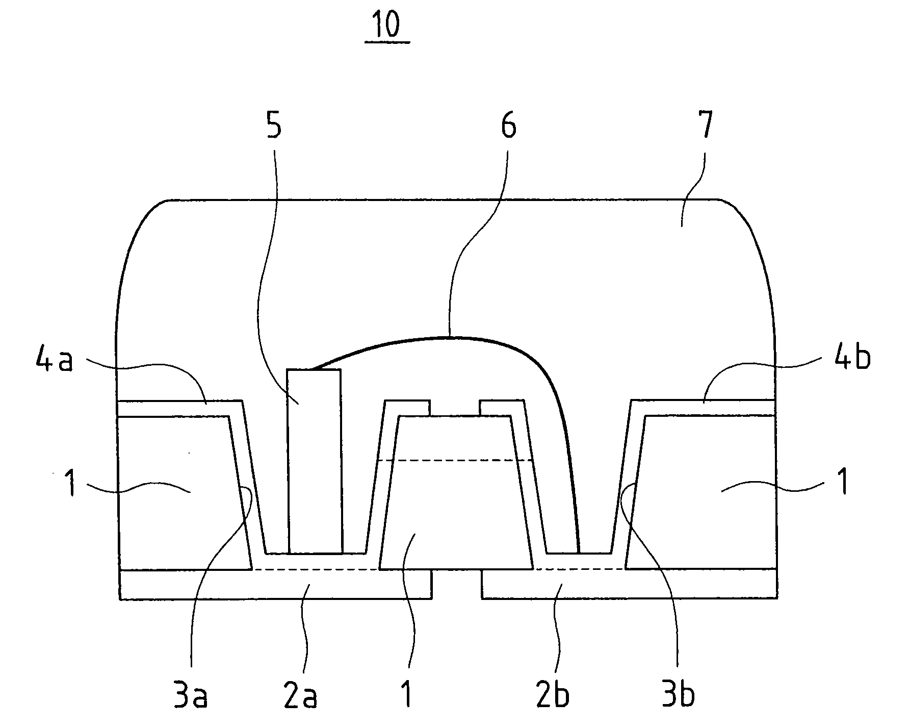
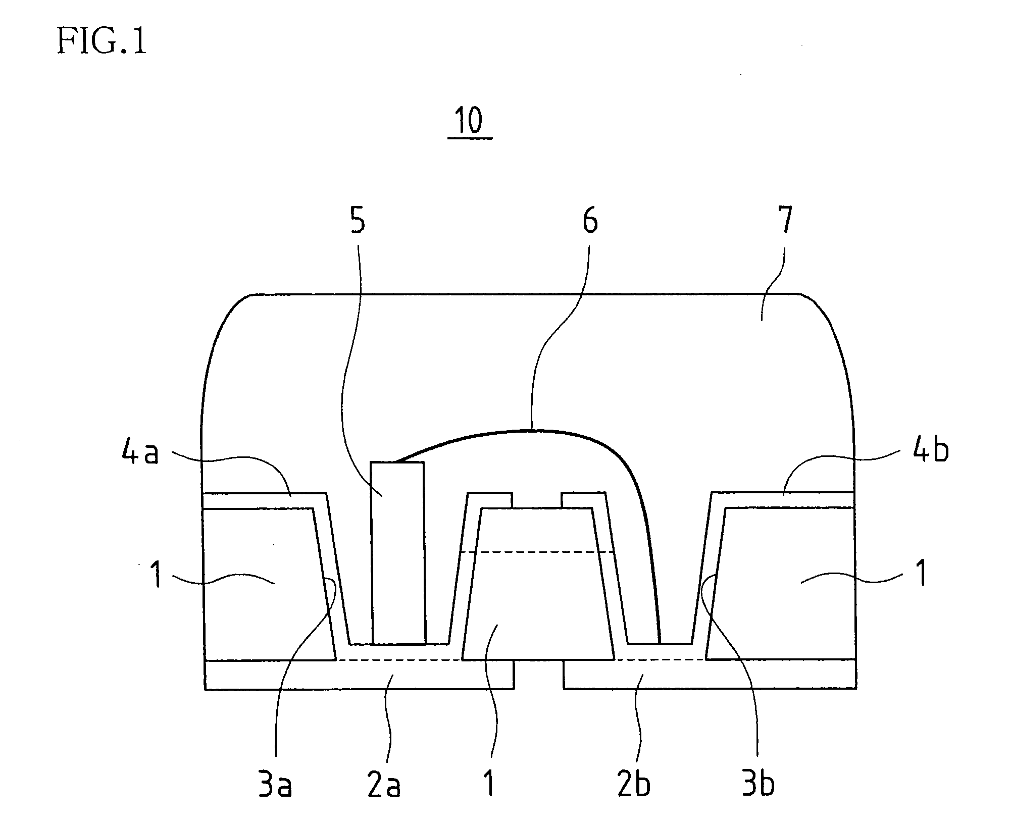
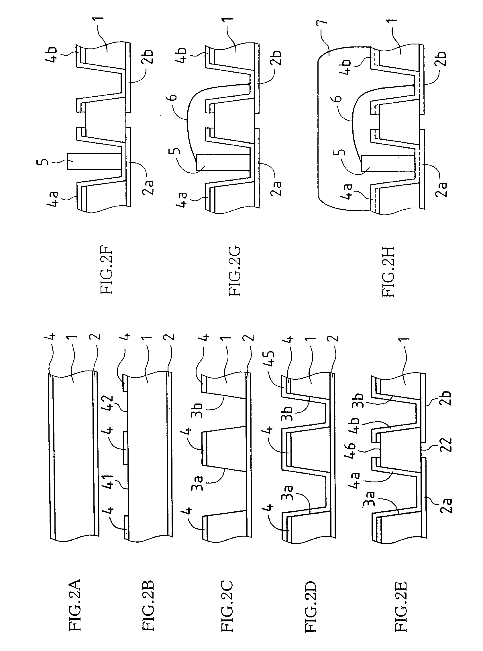
[0032]FIG. 1 is a cross-sectional view of a chip-type LED 10 according to the present first embodiment.

[0033]With the chip-type LED 10, a first concave hole (through-hole) 3a used for mounting an LED chip and a second concave hole (through-hole) 3b for connecting a metallic small-gauge wire are formed in an insulating substrate 1, and metallic (Cu) sheets 2a and 2b, which serve as the wiring patterns for the respective concave holes, are formed on the rear side of the insulating substrate 1 so as to be electrically separated from one another. A metallic sheet 4a, serving as a first wiring pattern at a portion that includes the first concave hole 3a, and a metallic sheet 4b, serving as a second wiring pattern at a portion that includes the second concave hole 3b, are formed on the front surface of the insulating substrate 1. Using this wiring structure, an LED chip 5 is mounted upon the metallic sheet 4a on the bottom surface portion of the first concave hole 3a, and the LED chip 5 i...

second embodiment

[0047]FIG. 3 is a cross-sectional view of a chip-type LED 20 according to the present second embodiment. In the following descriptions, members that are the same (or that have the same functionality) as those in the abovementioned first embodiment are given the same reference numerals.

[0048]With the chip-type LED 20, a first concave hole (through-hole) 3a used for mounting an LED chip is formed in an insulating substrate 1, and second and third concave holes (through-holes) 3b and 3c for connecting a metallic small-gauge wire are formed in the insulating substrate 1 on both sides of the first concave hole 3a. Metallic (Cu) sheets 2a, 2b, and 2c, which serve as the wiring patterns for the respective concave holes, are formed on the rear side of the insulating substrate 1 so as to be electrically separated from one another. A metallic sheet 4a, serving as a first wiring pattern at a portion that includes the first concave hole 3a, a metallic sheet 4b, serving as a second wiring patter...

third embodiment

[0062]FIGS. 5 and 6 are cross-section and plan views, respectively, of a chip-type LED 30 according to the third embodiment. In the following descriptions, members that are the same (or that have the same functionality) as those in the abovementioned first embodiment are given the same reference numerals.

[0063]With the chip-type LED 30, a first concave hole (through-hole) 3a used for mounting an LED chip and a second concave hole (through-hole) 3b for connecting a metallic small-gauge wire are formed in an insulating substrate 1, and metallic (Cu) sheets 2a and 2b, which serve as the wiring patterns for the respective concave holes, are formed on the rear side of the insulating substrate 1 so as to be electrically separated from one another. A metallic sheet 4a, serving as a first wiring pattern at a portion that includes the first concave hole 3a, and a metallic sheet 4b, serving as a second wiring pattern at a portion that includes the second concave hole 3b, are formed on the fro...


PUM


Abstract

An embodiment of the present invention has an insulating substrate in which a first concave hole for mounting an LED chip and a second concave hole for connecting a metallic small-gauge wire are formed, where a metallic sheet that serves as a first wiring pattern is formed at a portion that includes the first concave hole, a metallic sheet that serves as a second wiring pattern is formed at a portion that includes the second concave hole, an LED chip is mounted upon the metallic sheet inside the first concave hole, the LED chip is electrically connected to the metallic sheet inside the second concave hole via a metallic small-gauge wire, and the chip-type LED is sealed with a clear resin.

Description

BACKGROUND OF THE INVENTION[0001]This application claims priority under 35 U.S.C. §119(a) on Patent Application No. 2007-183342 filed in Japan on Jul. 12, 2007, the entire contents of which are herein incorporated by reference.[0002]The present invention relates to a surface-mounted chip-type LED and a method of manufacture thereof, used as a light source in various types of display panels, backlighting for liquid-crystal display devices, and in lighted switches and the like.[0003]Chip-type LEDs have conventionally been used as light sources in various types of display panels, backlighting for liquid-crystal display devices, and in lighted switches and the like.[0004]FIG. 8 illustrates an example of the structure of such a conventional chip-type LED.[0005]This conventional chip-type LED has a dual-layer structure using insulating substrates 81 and 82; a through-hole 83 is formed in the upper insulating substrate 82, and one wiring pattern 84 is formed so as to extend to the inside b...

Claims


Application Information

Patent Timeline
IPC IPC(8): H01L33/00H01L21/00H01L33/62H01L33/50H01L33/54H01L33/56H01L33/60
CPCH01L33/486H01L33/62H01L33/647H01L2224/45144H01L2224/48091H01L2224/48465H01L2224/73265H05K1/0203H05K1/183H05K2201/0394H05K2201/09509H05K2201/10106H05K2203/049H01L2924/00014H01L2924/00
Inventor MATSUDA, MAKOTO
Owner SHARP KK
Why Eureka
Try Eureka