Method and system for optoelectronics transceivers integrated on a CMOS chip

a technology of optoelectronics and transceivers, applied in the field of integrated circuit power control, can solve the problems of cable bulk penalties, large power requirements, and complex structure, and achieve only modest improvements in reach and limited scalability

Active Publication Date: 2009-01-22
CISCO TECH INC
View PDF17 Cites 115 Cited by
  • Summary
  • Abstract
  • Description
  • Claims
  • Application Information

AI Technical Summary

Benefits of technology

[0010]A system and/or method for optoelectronics transceivers integrated on a CMOS chip, substantially as shown

Problems solved by technology

They can be mitigated to some extent with equalization, coding, and shielding, but these techniques require considerable

Method used


Image

  • Method and system for optoelectronics transceivers integrated on a CMOS chip
  • Method and system for optoelectronics transceivers integrated on a CMOS chip
  • Method and system for optoelectronics transceivers integrated on a CMOS chip

Examples


Embodiment Construction

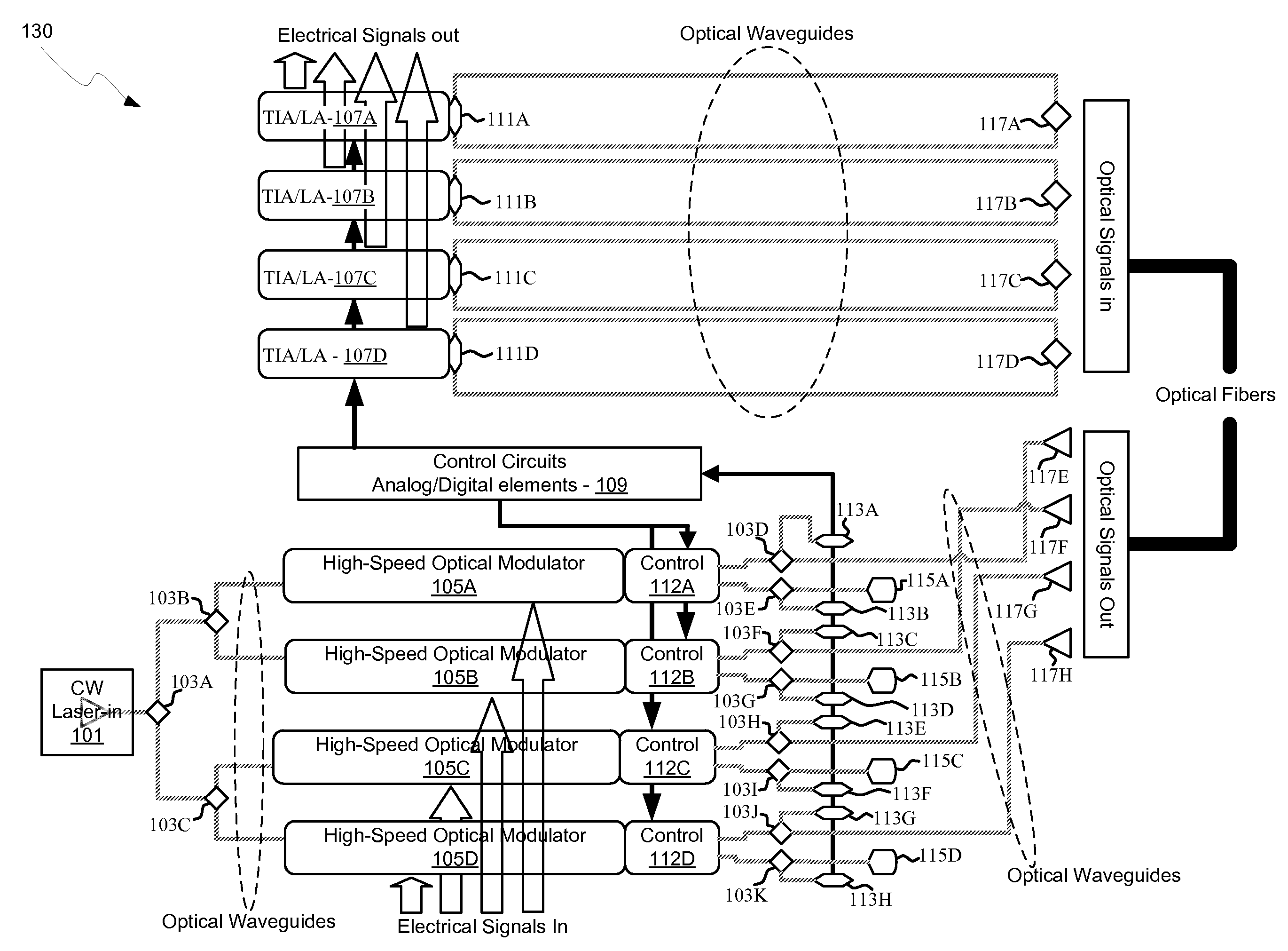
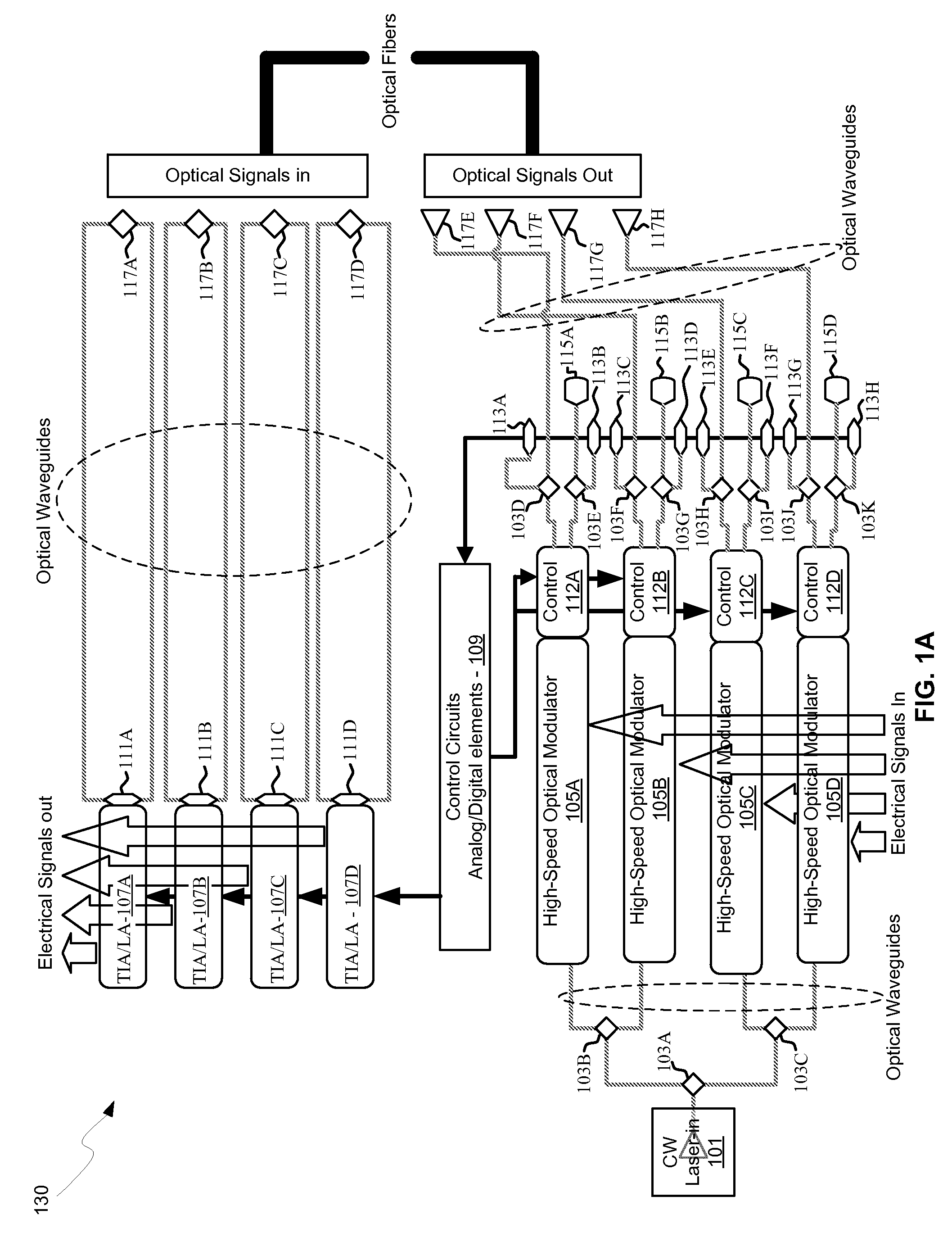
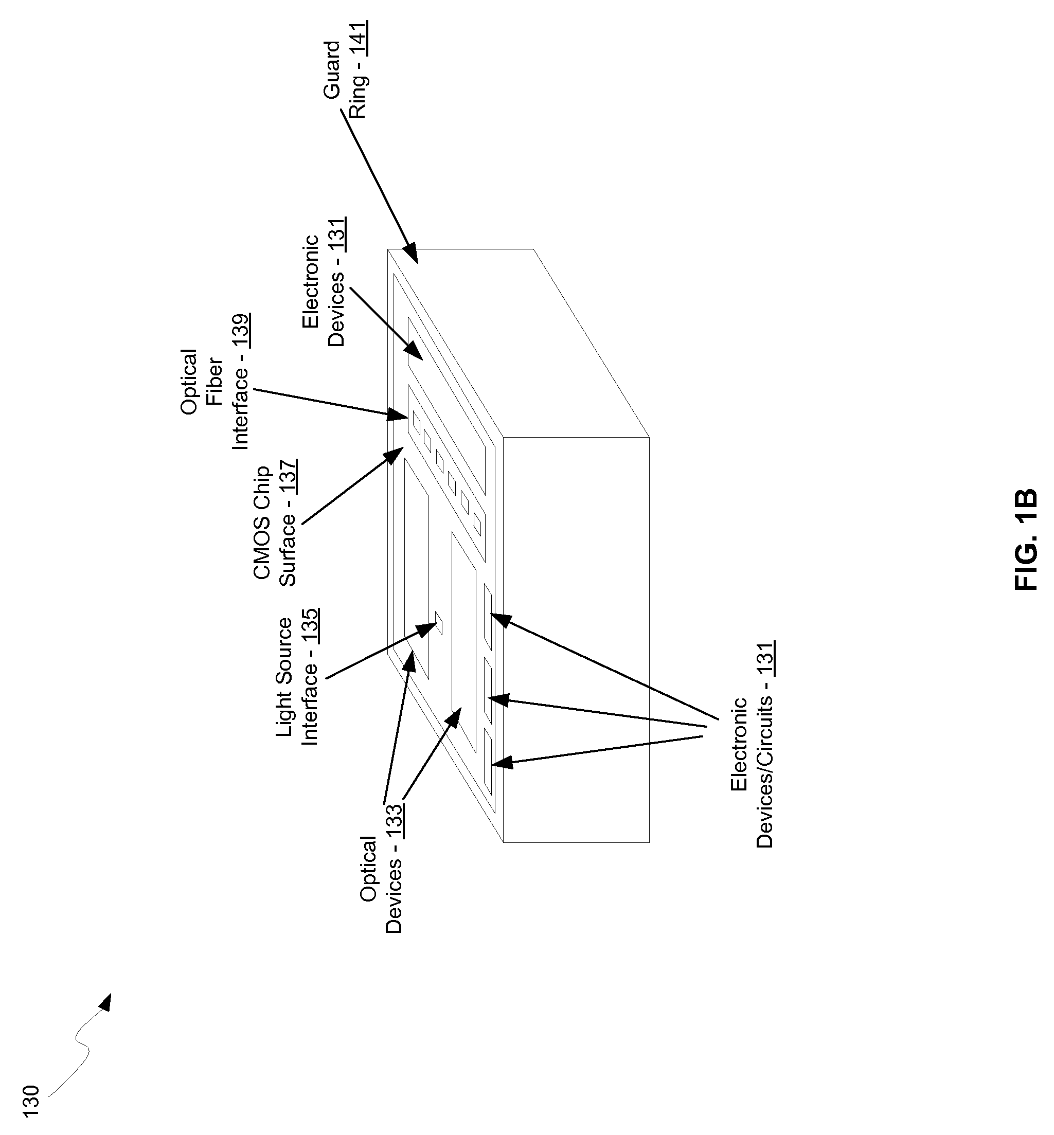
[0024]Certain aspects of the invention may be found in a method and system for optoelectronics transceivers integrated on a CMOS chip. Exemplary aspects of the invention may comprise receiving optical signals from one or more optical fibers via grating couplers on a top surface of a CMOS chip. The optical signals may be converted to electrical signals via one or more photodetectors integrated in or on the CMOS chip. The electrical signals may be processed via circuitry in the CMOS chip. A continuous-wave (CW) optical signal may be received from a laser source via grating couplers on the top surface of the CMOS chip, and may be modulated via one or more optical modulators integrated in or on the CMOS chip. Electrical signals may be received via the circuitry in the CMOS chip, and may drive the one or more optical modulators. The modulated optical signal may be communicated out of the top surface of the CMOS chip into one or more optical fibers via one or more grating couplers integra...


PUM


Abstract

Methods and systems for optoelectronics transceivers integrated on a CMOS chip are disclosed and may include receiving optical signals from optical fibers via grating couplers on a top surface of a CMOS chip, which may include a guard ring. Photodetectors may be integrated in the CMOS chip. A CW optical signal may be received from a laser source via grating couplers, and may be modulated using optical modulators, which may be Mach-Zehnder and/or ring modulators. Circuitry in the CMOS chip may drive the optical modulators. The modulated optical signal may be communicated out of the top surface of the CMOS chip into optical fibers via grating couplers. The received optical signals may be communicated between devices via waveguides. The photodetectors may include germanium waveguide photodiodes, avalanche photodiodes, and/or heterojunction diodes. The CW optical signal may be generated using an edge-emitting and/or a vertical-cavity surface emitting semiconductor laser.

Description

CROSS-REFERENCE TO RELATED APPLICATIONS / INCORPORATION BY REFERENCE[0001]This application makes reference to and claims priority to U.S. Provisional Application Ser. No. 61 / 057,127 filed on May 29, 2008, and Provisional Application Ser. No. 60 / 997,298 filed on Oct. 2, 2007, which are hereby incorporated herein by reference in their entirety.[0002]This application is also a continuation in part of U.S. patent application Ser. No. 11 / 611,084 filed on Dec. 14, 2006.[0003]This application also makes reference to U.S. Pat. Nos. 6,895,148; 7,039,258; 7,245,803; and 7,366,380.[0004]Each of the above stated applications and patents is hereby incorporated herein by reference in its entirety.FEDERALLY SPONSORED RESEARCH OR DEVELOPMENT[0005][Not Applicable]MICROFICHE / COPYRIGHT REFERENCE[0006][Not Applicable]FIELD OF THE INVENTION[0007]Certain embodiments of the invention relate to integrated circuit power control. More specifically, certain embodiments of the invention relate to a method and sy...

Claims


Application Information

Patent Timeline
IPC IPC(8): H04B10/00
CPCG02B6/1228G02B6/124H04B10/25G02B6/43G02B6/4214
Inventor PINGUET, THIERRYGLOECKNER, STEFFENABDALLA, SHERIFMIRSAIDI, SINADE DOBBELAERE, PETER
Owner CISCO TECH INC
Why Eureka
Try Eureka