
Vertical floating body cell of a semiconductor device and method for fabricating the same

Inactive Publication Date: 2009-01-29
SK HYNIX INC
View PDF3 Cites 138 Cited by
  • Summary
  • Abstract
  • Description
  • Claims
  • Application Information

AI Technical Summary

Benefits of technology

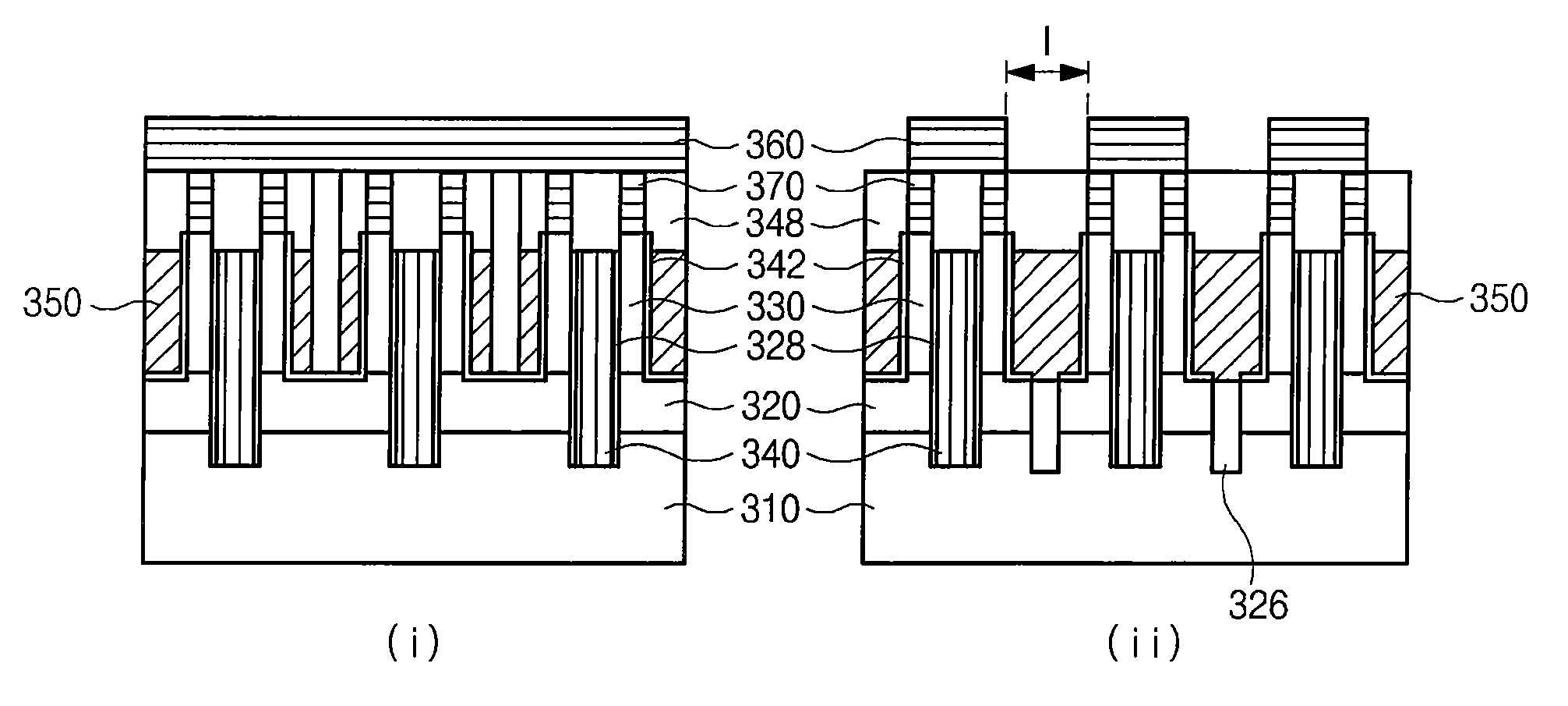
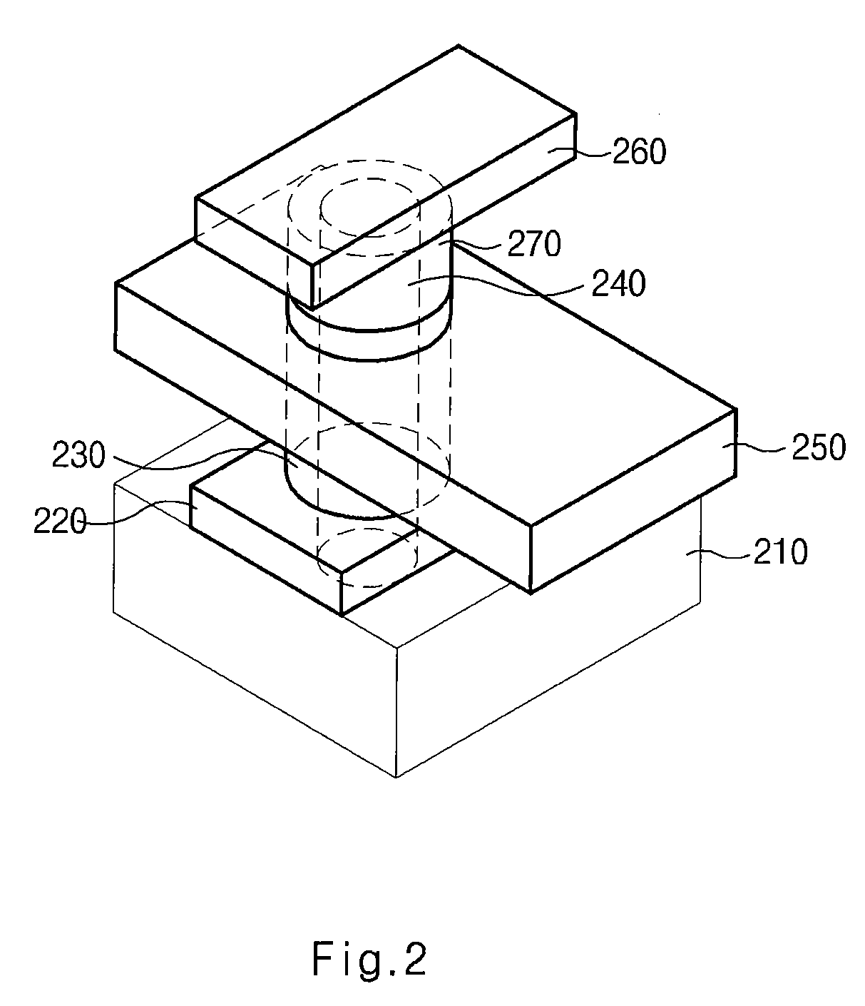
[0007]Embodiments of the present invention are directed to a semiconductor device including a FBC. According to an embodiment of the invention, the FBC includes a tube-type channel, a bias electrode connected to a semiconductor substrate in the tube-type channel, an insulating film disposed between the tube-type channel and the bias electrode, and a surrounding gate formed over the tube-type channel. The FBC secures a sufficient area where charges are accumulated, thereby improving integration of the device and data retention time of the device.

Problems solved by technology

In DRAM a capacitor is connected to a cell transistor, and a complicated process is required to form the structure.
Also, generated charges are recombined into source / drain regions so that it is difficult to retain data.
As a result, it is difficult to reduce the size of the transistor.
The usage of the SOI wafer increases manufacturing costs, thereby limiting commercialization of FBCs.

Method used


Image

  • Vertical floating body cell of a semiconductor device and method for fabricating the same
  • Vertical floating body cell of a semiconductor device and method for fabricating the same
  • Vertical floating body cell of a semiconductor device and method for fabricating the same

Examples


Embodiment Construction

[0014]According to an embodiment of the present invention, a semiconductor device has a FBC structure which includes a vertical transistor.

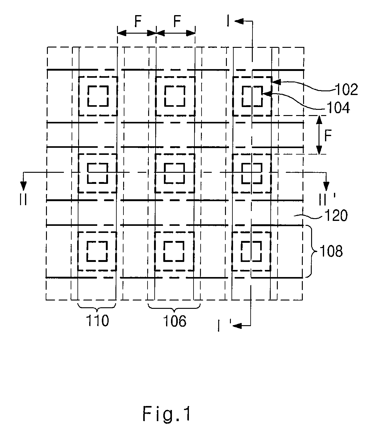
[0015]FIG. 1 is a layout of a semiconductor device according to an embodiment of the present invention. A semiconductor device includes a channel region 102 defined by a device isolation region 120, a bias electrode region 104, a source line region 106, a word line region 108, and a bit line region 110. Source line region 106 is extended toward one direction over a semiconductor substrate. Channel region 102 is disposed over source line region 106 to have a vertical tube structure. Bias electrode region 104 is located in channel region 102.

[0016]An outer line-width of channel region 102 is F, where F is a distance between two adjacent channel regions 102. Although the top surface of channel region 102 (as shown in FIG. 1) is formed to be rectangular in the embodiment of the present invention, the top surface of channel region 102 may be formed to...


PUM


Abstract

A semiconductor device includes a tube-type channel formed over a semiconductor substrate. The tube-type channel is connected to first and second conductive lines. A bias electrode is formed in the tube-type channel. The bias electrode is connected to the semiconductor substrate. An insulating film is disposed between the tube-type channel and the bias electrode. A surrounding gate electrode is formed over the tube-type channel.

Description

CROSS-REFERENCES TO RELATED APPLICATIONS[0001]This application claims priority of Korean patent application number 10-2007-0075590, filed on Jul. 27, 2007, which is incorporated by reference in its entirety.BACKGROUND OF THE INVENTION[0002]The invention generally relates to a semiconductor device. More particularly, the invention relates to a vertical floating body cell and a method for fabricating the same.[0003]Efforts have been made to overcome limitations of a cell structure including a transistor and a capacitor. For example, a capacitor that inhibits the high integration of a memory is eliminated, and a memory cell is configured to have a transistor, which is referred to as a floating body cell (FBC) structure. The FBC structure utilizes a floating body effect phenomenon that changes a threshold voltage when charges are accumulated in a channel bottom of the transistor.[0004]When holes are injected or accumulated into a NMOS, a floating body effect is generated to lower the th...

Claims


Application Information

Patent Timeline
IPC IPC(8): H01L29/78H01L21/336
CPCH01L21/84H01L29/7841H01L27/1203H01L27/10802H10B12/20H10B99/00H10B12/00
Inventor CHUNG, SUNG WOONG
Owner SK HYNIX INC
Learn More