Light-emitting element, light-emitting device, and vapor deposition apparatus

a technology of light-emitting devices and vapor deposition apparatus, which is applied in the direction of organic semiconductor devices, discharge tubes/lamp details, discharge tubes luminescnet screens, etc., and can solve problems such as difficulty in changing electrical characteristics without changing optical characteristics

Inactive Publication Date: 2009-01-29
SEMICON ENERGY LAB CO LTD
View PDF28 Cites 14 Cited by
  • Summary
  • Abstract
  • Description
  • Claims
  • Application Information

AI Technical Summary

Benefits of technology

[0028]One feature of the invention is to provide a light-emitting element including a pair of electrodes, and a layer containing a light-emissive substance sandwiched therebetween. Based on an image observed with a transmission electron microscope, the layer containing a light-emissive substance has a stack where a region having a high average atomic weight and a region having a low average atomic weight are alternately stacked, and the thickness of the stack is not less than 0.5 nm and not more than 30 nm. Note that a region having a high average atomic weight and a region having a low average atomic weight are called a region having a concentration an inorganic compound higher than a concentration of an organic compound and a region having a concentration an inorganic compound lower than a concentration of an organic compound in this specification.
[0029]One feature of the invention of this specification is to provide a light-emitting element including a pair of electrodes, and a layer containing a light-emissive substance sandwiched therebetween. Based on an image observed with a transmission electron microscope, the layer containing a light-emissive substance has a stack where a region having a high average atomic weight and a region having a low average atomic weight are alternately stacked, and the thickness of the stack is not less than 1 nm and not more than 10 nm.
[0030]One feature of the invention of this specification is to provide a light-emitting element including a pair of electrodes and a layer containing a light-emissive substance sandwiched therebetween. Based on an image observed with a transmission electron microscope, the layer containing a light-emissive substance has a stack where a region with a dark color and a region with a light color are alternately stacked, and the thickness of the stack is not less than 0.5 nm and not more than 30 nm.
[0031]One feature of the invention of this specification is to provide a light-emitting element including a pair of electrodes and a layer containing a light-emissive substance sandwiched therebetween. Based on an image observed with a transmission electron microscope, the layer containing a light-emissive substance has a stack where a region with a dark color and a region with a light color are alternately stacked, and the thickness of the stack is not less than 1 nm and not more than 10 nm.

Problems solved by technology

Thus, it has been difficult to change the electrical characteristics without changing the optical characteristics.

Method used


Image

  • Light-emitting element, light-emitting device, and vapor deposition apparatus
  • Light-emitting element, light-emitting device, and vapor deposition apparatus
  • Light-emitting element, light-emitting device, and vapor deposition apparatus

Examples


embodiment mode 1

[0060]In this embodiment mode, description is made on a layer containing a composite material which is included in the light-emitting element of the invention.

[0061]The layer containing a composite material includes an organic compound and an inorganic compound, and the concentration ratio of the organic compound to the inorganic compound changes periodically. Since the concentration ratio of the organic compound to the inorganic compound changes periodically, conductivity in a stacked direction (also called a thickness direction) can be controlled. The “stacked direction” in this specification means a direction in one electrode of electrodes at the both side of the layer containing the composite material from the other electrode of the electrodes.

[0062]By changing the length of a cycle in which the concentration ratio of the organic compound to the inorganic compound changes periodically, a layer having desired conductivity can be obtained. For example, conductivity in the stacked ...

embodiment mode 2

[0085]Description is made with reference to FIG. 20 to FIG. 23 on a vapor deposition apparatus used for carrying out the invention, and a method for forming a layer containing a composite material by using the vapor deposition apparatus.

[0086]A vapor deposition apparatus used for carrying out the invention is provided with a processing chamber 1001 where vapor deposition is performed with respect to an object to be processed, and a transfer chamber 1002. The object to be processed is transferred to the processing chamber 1001 through the transfer chamber 1002. The transfer chamber 1002 is provided with an arm 1003 for transferring the object to be processed (FIG. 23).

[0087]Inside the processing chamber 1001, a holding portion for holding the object to be processed, an evaporation source 1011a for holding a first material, and an evaporation source 1011b for holding a second material are provided as shown in FIG. 20. In FIG. 20, the holding portion for holding the object to be proces...

embodiment mode 3

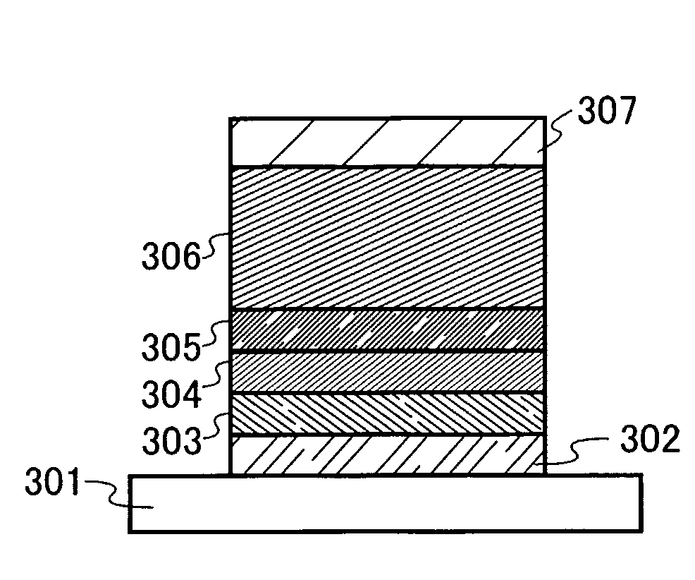
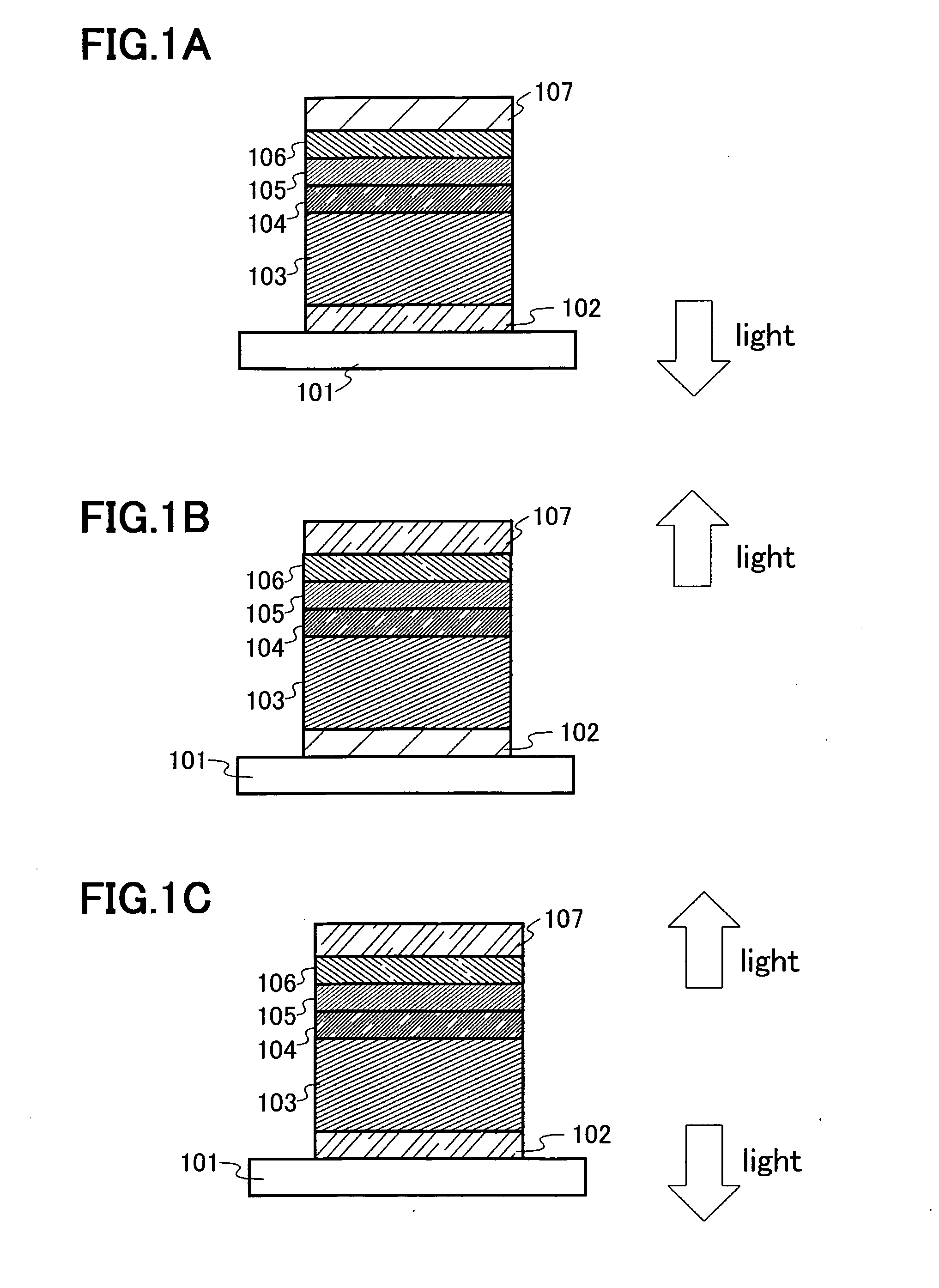
[0103]A light-emitting element of the invention has a plurality of layers between a pair of electrodes. The plurality of layers are formed by stacking layers each formed of a substance with a high carrier injection property or a high carrier transporting property so that a light-emitting region is provided away from the electrodes, that is, carriers may be recombined in a portion away from the electrodes.

[0104]Description is made below with reference to FIG. 1A on one mode of the light-emitting element of the invention.

[0105]In this embodiment, the light-emitting element is formed by stacking a first electrode 102, a first layer 103, a second layer 104, a third layer 105, a fourth layer 106, and a second electrode 107 in this order. Note that in this embodiment mode, description is made below on the assumption that the first electrode 102 functions as an anode while the second electrode 107 functions as a cathode.

[0106]A substrate 101 is used as a support of the light-emitting eleme...


PUM

PropertyMeasurementUnit
thicknessaaaaaaaaaa
thicknessaaaaaaaaaa
thicknessaaaaaaaaaa

Abstract

To provide a light-emitting element and a light-emitting device which can be designed and manufactured with redundancy. A light-emitting element of the invention includes a pair of electrode, and a layer containing a light-emissive substance between the pair of electrodes. The layer containing a light-emissive substance includes a layer containing a composite material, and the layer containing a composite material includes an organic compound and an inorganic compound. The concentration ratio of the organic compound to the inorganic compound changes periodically. The layer containing a composite maternal can be changed in electrical characteristics without changing the composition ratio of the organic compound to the inorganic compound in the layer or changing the kind of compounds used for the layer.

Description

TECHNICAL FIELD[0001]The present invention relates to a light-emitting element utilizing electroluminescence and a light-emitting device having the light-emitting element, and an apparatus for manufacturing the light-emitting device.BACKGROUND ART[0002]In recent years, light-emitting elements using light-emissive organic compounds have actively been researched and developed. Such light-emitting elements basically have a structure where a layer containing a light-emissive organic compound is sandwiched between a pair of electrodes. By applying a voltage to such elements, electrons and holes are respectively injected into the layer containing a light-emissive organic compound from the pair of electrodes, and thus current flows therein. Then, these carriers (electrons and holes) are recombined with each other to bring the light-emissive organic compound into an excited state. The light-emissive organic compound emits light upon returning from the excited state to the ground state. Beca...

Claims


Application Information

Patent Timeline
Patent Type & Authority Applications(United States)
IPC IPC(8): H01J1/62C23C16/00
CPCC23C14/044C23C14/24C23C14/505C23C14/548H01L51/001H05B33/22H01L51/5052H01L51/5088H01L2251/5315H01L2251/5323H05B33/10H01L51/006H10K71/164H10K85/633H10K50/155H10K50/165H10K50/17H10K2102/3031H10K2102/3026
Inventor IKEDA, HISAOSAKATA, JUNICHIROSEO, SATOSHIIWAKI, YUJI
Owner SEMICON ENERGY LAB CO LTD
Why Eureka
Try Eureka