Organic elecroluminescence display apparatus, method of producing the same, and method of repairing a defect

a technology of electroluminescence display and organic light, which is applied in the direction of electrical devices, instruments, semiconductor devices, etc., can solve the problems of large number of non-lighting pixels, large amount of non-lighting pixels, and small thickness of organic light emitting layer formed between electrodes, etc., and achieves a small amount of current flowing through the panel and hardly increasing costs.

Inactive Publication Date: 2007-11-29
CANON KK
View PDF5 Cites 186 Cited by
  • Summary
  • Abstract
  • Description
  • Claims
  • Application Information

AI Technical Summary

Benefits of technology

[0032]According to the present invention, after a defective portion is detected, a current is caused to flow through only the defective portion, so a normal pixel is not degraded. Further, a current flowing through a panel is suppressed greatly as compared with a case where a current is caused to flow through the whole pixels. Therefore, device degradat...

Problems solved by technology

In the organic EL display, in a case where the anode electrode and the cathode electrode interposing the organic light emitting layer are short-circuited, an organic EL device in that portion does not emit light, with the result that a non-lighting defect occurs.
Generally, the thickness of the organic light emitting layer formed between the electrodes is very small, that is, about several 10 nm to 100 nm, and a large number of non-lighting pixels are likely to be caused by the short-circuit between the electrodes.
In the organic EL display, it is very difficult to prevent foreign matters of a sub-micron or less from adhering to an inside of a surface of a display, so there is a demand for the countermeasure against a non-lighting pixel.
However, it is difficult to find in which place of a pi...

Method used


Image

  • Organic elecroluminescence display apparatus, method of producing the same, and method of repairing a defect
  • Organic elecroluminescence display apparatus, method of producing the same, and method of repairing a defect
  • Organic elecroluminescence display apparatus, method of producing the same, and method of repairing a defect

Examples


embodiment 1

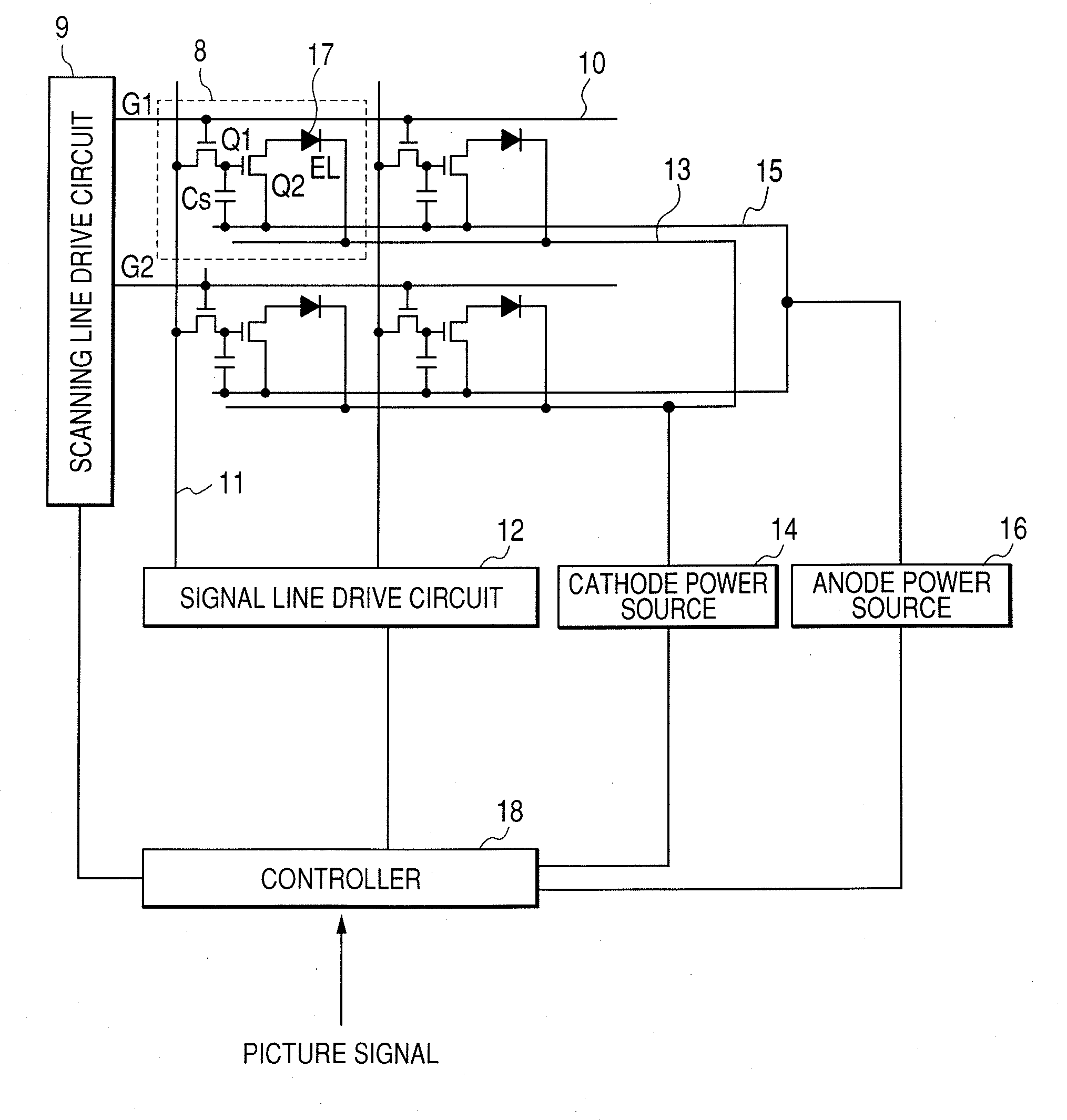
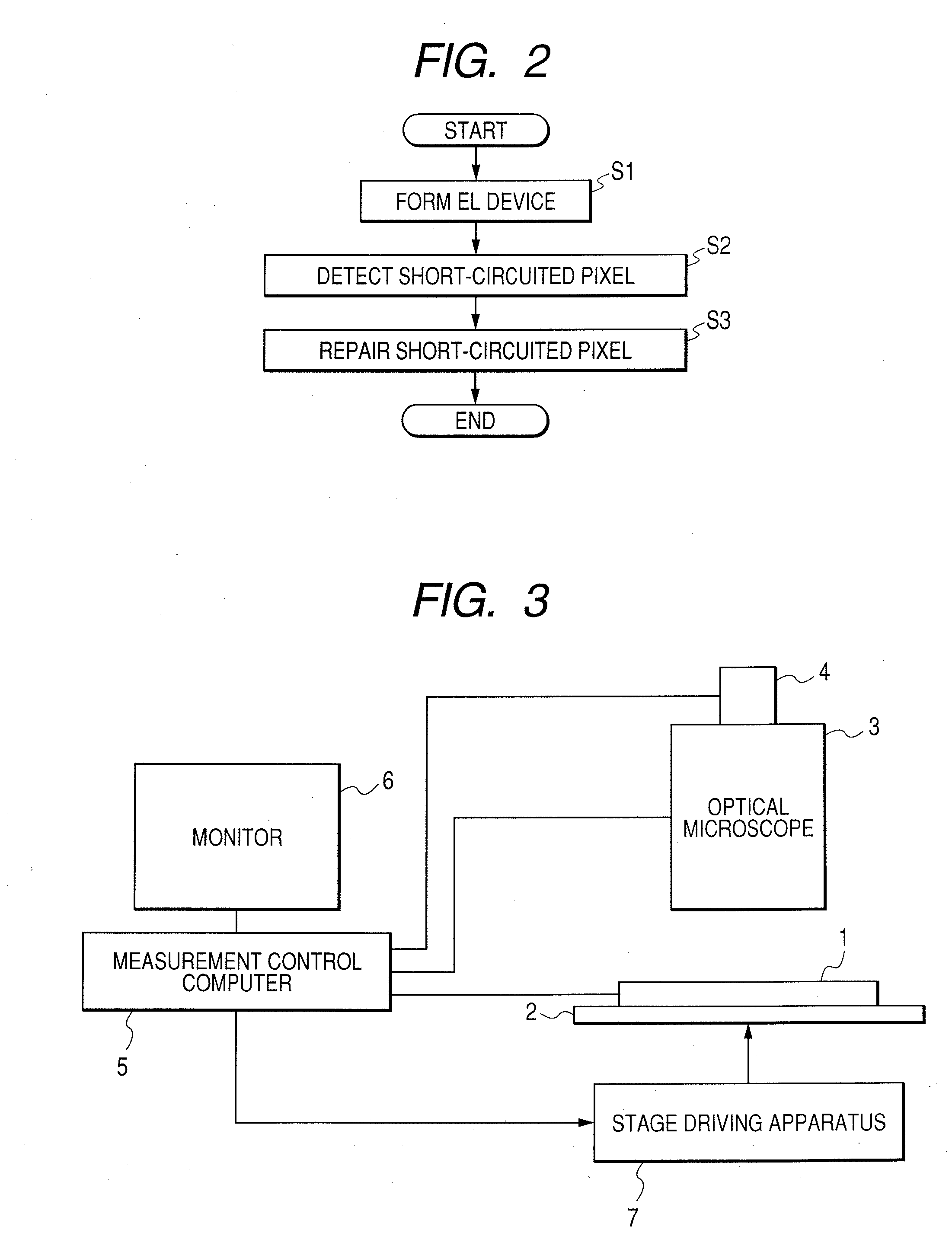
[0053]First, referring to FIGS. 1 to 5, Embodiment 1 of the present invention will be described. FIG. 1 is a block diagram illustrating an organic EL display apparatus according to this embodiment, and FIG. 2 is a flowchart schematically illustrating a production method thereof.

[0054]In the organic EL display apparatus illustrated in FIG. 1, in a pixel matrix array region on an insulating substrate (active matrix substrate), pixels 8 made of organic EL light emitting devices and drive circuits thereof are arranged in a matrix array. Each of the pixels 8 has a switching transistor (TFT) Q1 playing a role as a switch for selecting a pixel, a holding capacitor Cs, an operation transistor (TFT) Q2 supplying a current to an EL device, and an organic EL device 17. Further, on the insulating substrate (active matrix substrate), a plurality of scanning lines (gate lines) 10 is provided along a row direction, and a plurality of signal lines 11 is provided along a column direction. In the exa...

embodiment 2

[0091]Next, referring to FIGS. 6 to 8, Embodiment 2 of the present invention will be described.

[0092]In this embodiment, a method of electrically detecting a defective pixel will be described without using an optical microscope in a defective pixel detection step, unlike Embodiment 1.

[0093]FIG. 6 is a schematic diagram of an inspection apparatus serving as a repair apparatus used in a step of specifying a defective pixel and a repair step in the method of producing an organic EL display apparatus according to this embodiment. FIG. 7 is a flowchart schematically illustrating a production method using the inspection apparatus. The configuration of the organic EL display apparatus of this embodiment is the same as that of Embodiment 1, so the description thereof will be omitted.

[0094]The inspection apparatus illustrated in FIG. 6 includes a measurement control computer 21 and a monitor 22 connected to an organic EL display apparatus 20, and a current measuring unit 23 connected to the ...

embodiment 3

[0110]Next, referring to FIG. 9, Embodiment 3 of the present invention will be described. FIG. 9 is a flowchart schematically illustrating a method of producing an organic EL display apparatus according to this embodiment. The configuration of the organic EL display apparatus of this embodiment is the same as that in Embodiment 1 except for a repair method.

[0111]In FIG. 9, after an EL device is formed in the same way as described above (Step S31), a current is allowed to flow between a cathode electrode and an anode electrode of an n-th pixel (Step S32). A defect is determined based on the measurement results, and the positional data (coordinate value) of a short-circuited pixel is stored (Step S33). This operation is repeated until the determination of a defect with respect to all the pixels is completed (Step S34). After that, a voltage is applied to the short-circuited pixel for a predetermined period of time, thereby repairing the short-circuited pixel. After that, the lighting ...


PUM


Abstract

Provided is an organic EL display apparatus capable of opening and breaking a defective portion without degrading a normal portion of a pixel, and a method of producing the same. The method of producing an organic EL display apparatus in which a plurality of pixels including organic EL devices are arranged includes the steps of: forming an organic EL device formed of a light emitting layer made of an organic compound between a cathode electrode and an anode electrode (Step S1); detecting a defective pixel in which a cathode electrode and an anode electrode are short-circuited (Step 2); and repairing the defective pixel to be opened by selectively applying a voltage between the cathode electrode and the anode electrode with respect to the defective pixel (Step S3).

Description

BACKGROUND OF THE INVENTION[0001]1. Field of the Invention[0002]The present invention relates to an organic electroluminescence (EL) display apparatus, a method of producing the same, a method of repairing a defect, and a repair apparatus. In particular, the present invention relates to a method of selectively repairing a pixel having a defective portion in which a cathode electrode and an anode electrode of an organic EL device are short-circuited, so as to enhance a yield of a repair display.[0003]2. Description of the Related Art[0004]In recent years, an EL display apparatus (organic EL display) has been developed actively, which is capable of being made thinner than a cathode ray tube (CRT), obtaining a wider viewing angle than a liquid crystal display apparatus, and being reduced in weight and cost.[0005]The organic EL display generally has a configuration in which an organic light emitting layer is interposed between an anode electrode and a cathode electrode, and light is emi...

Claims


Application Information

Patent Timeline
IPC IPC(8): G09G3/10
CPCG09G3/006G09G3/3225H01L2251/568G09G2320/043G09G2330/08G09G2320/0223H10K71/861
Inventor NAGAYAMA, KOHEI
Owner CANON KK
Why Eureka
Try Eureka