Symmetric bidirectional silicon-controlled rectifier

Active Publication Date: 2009-02-05
AMAZING MICROELECTRONICS
View PDF7 Cites 85 Cited by
  • Summary
  • Abstract
  • Description
  • Claims
  • Application Information

AI Technical Summary

Benefits of technology

[0006]The primary objective of the present invention is to provide a symmetric bidirectional silicon

Problems solved by technology

The submicron or deep-submicron technology uses so thin a gate oxide layer that only a few volts higher voltage is enough to cause gate oxide damage.
In general environments, electrostatic voltage maybe reach thousands or even several ten thousands volts, which will damage integrated circuits (IC).
As the silicon-controlled rectifi

Method used


Image

  • Symmetric bidirectional silicon-controlled rectifier
  • Symmetric bidirectional silicon-controlled rectifier
  • Symmetric bidirectional silicon-controlled rectifier

Examples


Embodiment Construction

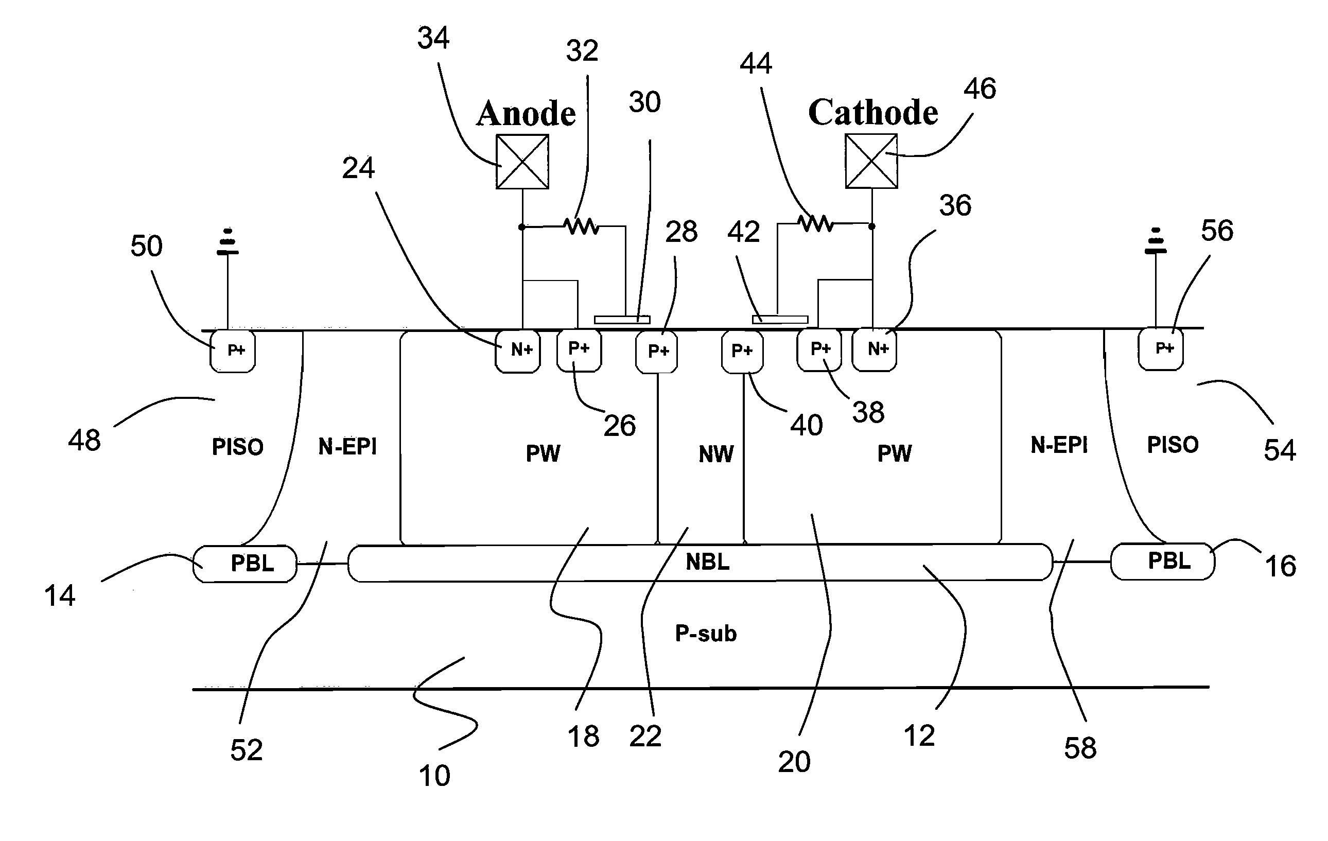
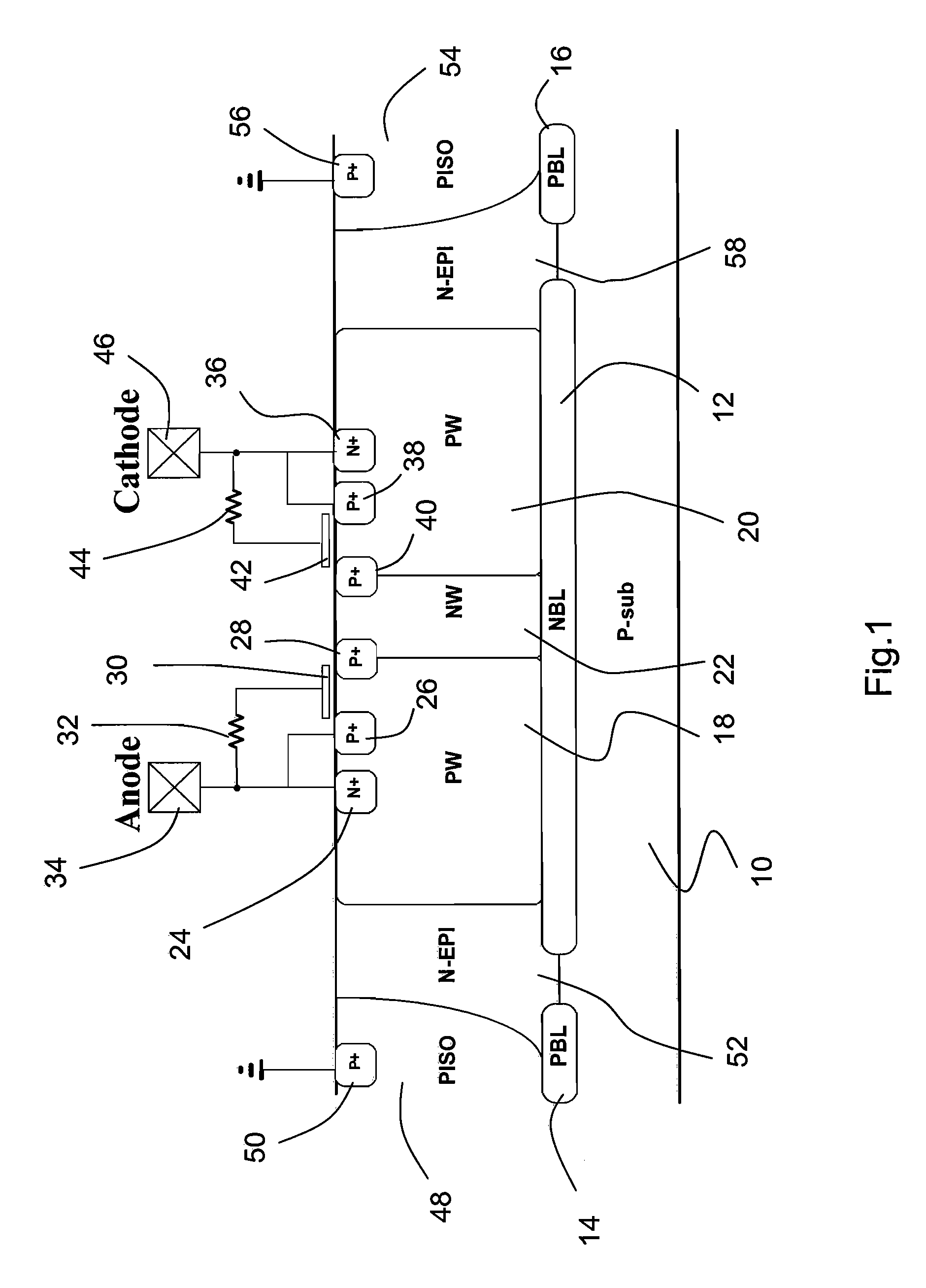
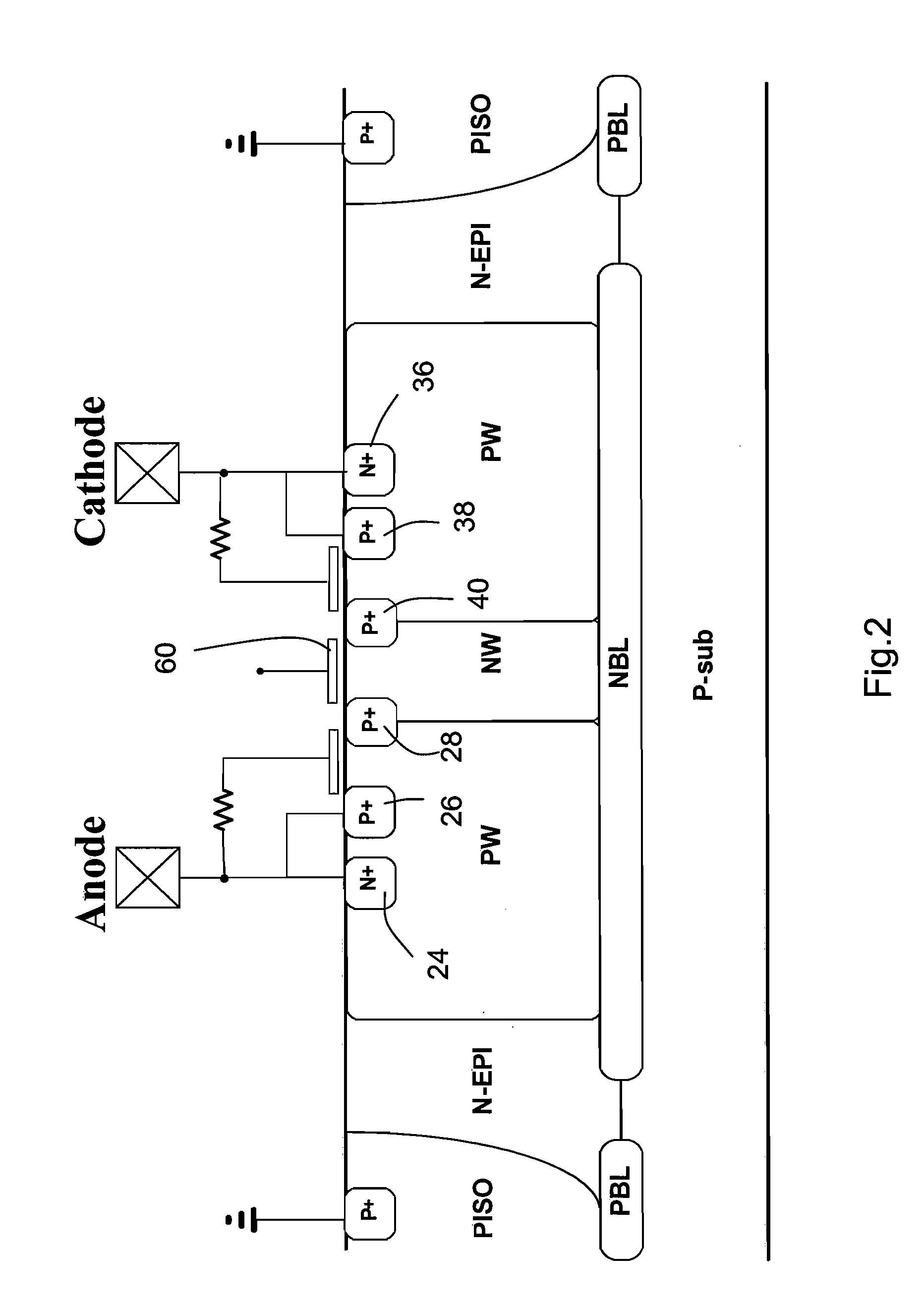
[0023]Refer to FIG. 1 a diagram schematically showing an embodiment of a symmetric silicon-controlled rectifier according to the present invention. In this embodiment, the symmetric silicon-controlled rectifier of the present invention comprises: a P-type substrate 10; an N-type first buried layer 12 formed on the substrate 10; and P-type second and third buried layer 14 and 16 respectively formed at two sides of the first buried layer 12.

[0024]A P-type first well 18, a middle region 22 and a P-type second well 20 are side-by-side formed on the first buried layer 12. The middle region 22 is interposed between the first and second wells 18 and 20 and may be an undoped epitaxial region or an arbitrary N-type region, such as an N-type epitaxial region or an N-type well. An N-type first semiconductor area 24 and a P-type second semiconductor area 26 are both formed inside the first well 18. A P-type third semiconductor area 28 is formed in a junction between the first well 18 and the mi...


PUM


Abstract

The present invention discloses a symmetric bidirectional silicon-controlled rectifier, which comprises: a substrate; a buried layer formed on the substrate; a first well, a middle region and a second well, which are sequentially formed on the buried layer side-by-side; a first semiconductor area and a second semiconductor area both formed inside the first well; a third semiconductor area formed in a junction between the first well and the middle region, wherein a first gate is formed over a region between the second and third semiconductor areas; a fourth semiconductor area and a fifth semiconductor area both formed inside the second well; a sixth semiconductor area formed in a junction between the second well and the middle region, wherein a second gate is formed over a region between the fifth and sixth semiconductor areas.

Description

BACKGROUND OF THE INVENTION[0001]1. Field of the Invention[0002]The present invention relates to a silicon-controller rectifier, particularly to a symmetric bidirectional silicon-controlled rectifier, which has a small area and a high electrostatic-discharge protection capability. The present invention applies to an ESD protection element for I / O signals with both positive and negative voltage level.[0003]2. Description of the Related Art[0004]With the advance of semiconductor technology, the dimensions of MOS (Metal Oxide Semiconductor) devices have been reduced to a submicron or even deep-submicron scale. The submicron or deep-submicron technology uses so thin a gate oxide layer that only a few volts higher voltage is enough to cause gate oxide damage. In general environments, electrostatic voltage maybe reach thousands or even several ten thousands volts, which will damage integrated circuits (IC). Therefore, once having accumulated to a given amount in IC, electrostatic charge s...

Claims


Application Information

Patent Timeline
IPC IPC(8): H01L29/747
CPCH01L27/0262H01L29/87H01L29/747
Inventor TSENG, TANG-KUEICHUANG, CHE-HAOJIANG, RYAN HSIN-CHINKER, MING-DOU
Owner AMAZING MICROELECTRONICS
Why Eureka
Try Eureka