Methods of fabricating dual fin structures and semiconductor device structures with dual fin structures
a technology of dual fins and fin structures, applied in the direction of semiconductor devices, electrical equipment, basic electric elements, etc., can solve the problems of increasing the problem of short channel effects attributable to shortened channel lengths
- Summary
- Abstract
- Description
- Claims
- Application Information
AI Technical Summary
Problems solved by technology
Method used
Image
Examples
Embodiment Construction
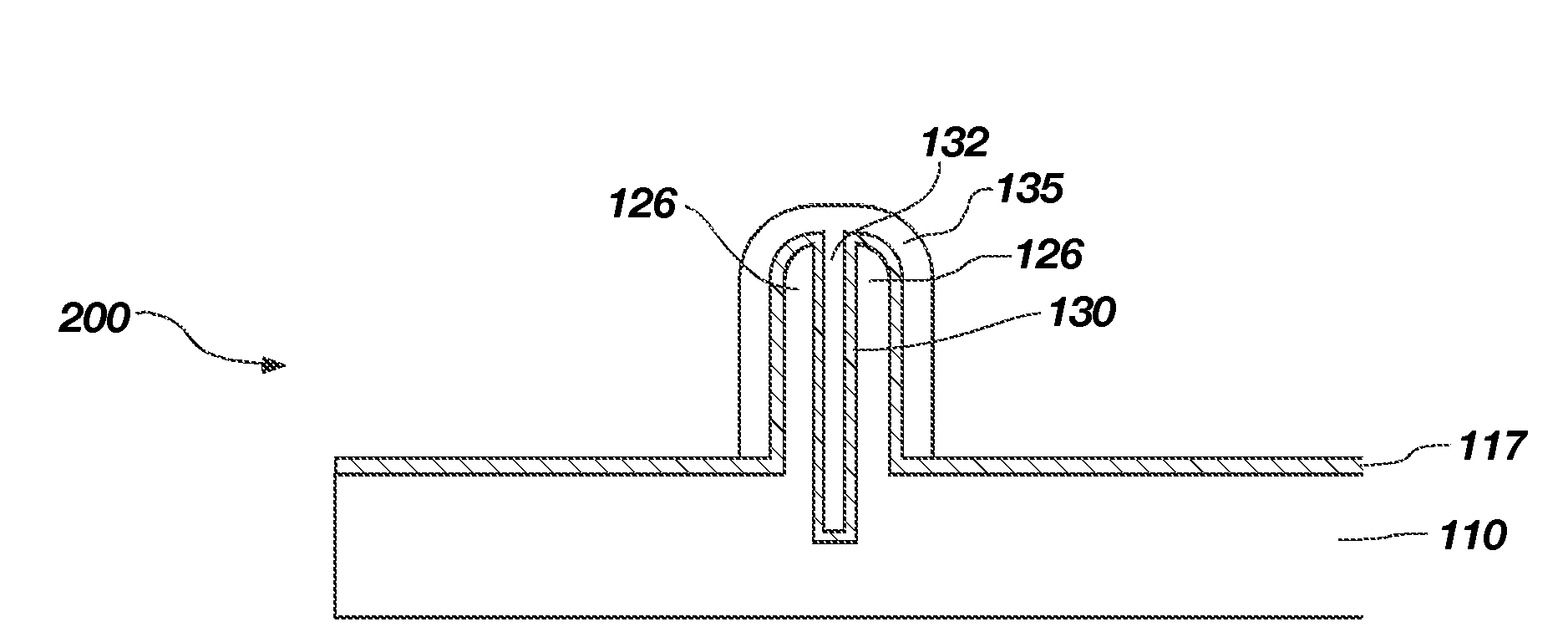
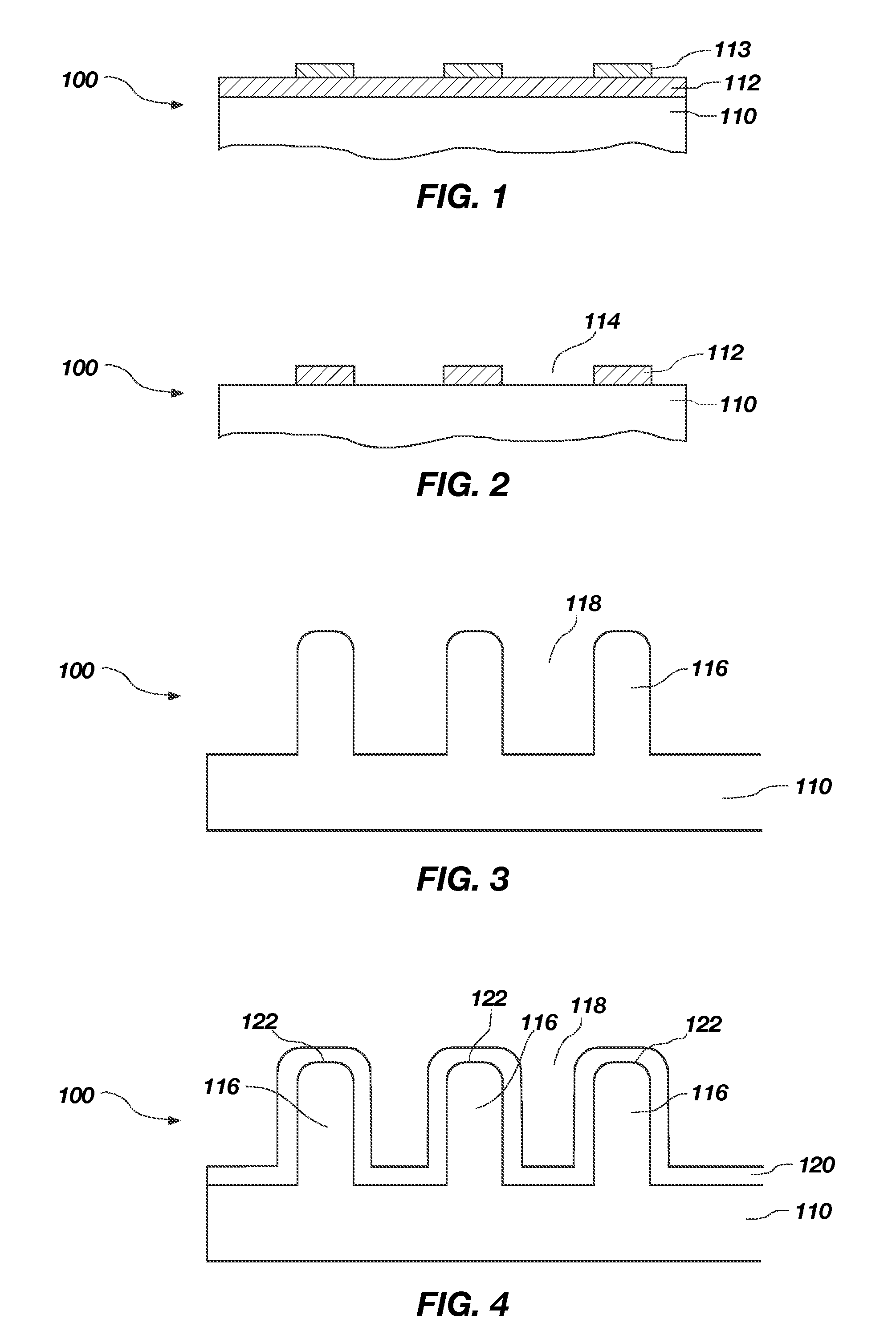
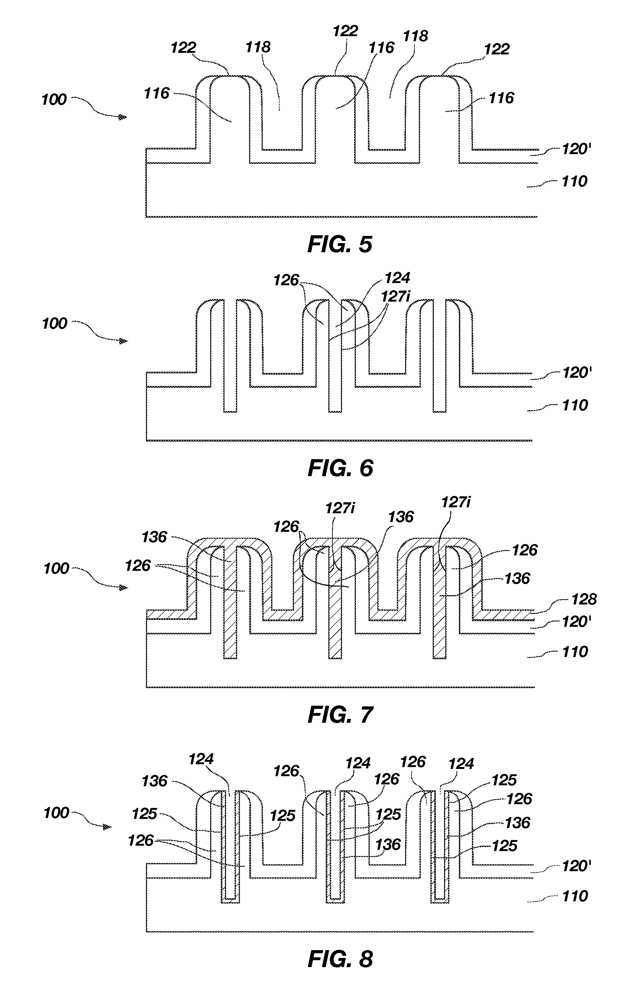
[0009]Embodiments of methods for fabricating semiconductor device structures with dual fins are disclosed, as are embodiments of semiconductor device structures including dual fin-FETs, and systems incorporating same. As used herein, the term “fin” includes a semiconducting material which is etched into a substantially vertically extending structure, relative to a major plane of a substrate on which the structure is formed, that will form the active regions of a semiconductor device such as source, drain and trench. The methods disclosed herein may be used to fabricate a variety of devices such as dynamic random access memory (DRAM) devices, CMOS devices, and other devices in which fin-FETs would be suitable and increases in drive current are desired.
[0010]Reference will now be made to the figures wherein like numerals represent like elements. The figures are not necessarily drawn to scale. Elements in the figures are drawn in cross-section.
[0011]FIGS. 1-6 depict, in simplified cros...
PUM
 Abstract
Description
Claims
Application Information


