Liquid crystal device

a liquid crystal device and liquid crystal technology, applied in the field of liquid crystal devices, can solve the problems of difficult to determine in which image portion of the pointing object the image portion of the pointing object is located, and the shadow of the other portion cannot be distinguished from each other, so as to reduce the aperture ratio of the display area and accurate positioning

Active Publication Date: 2009-02-05
JAPAN DISPLAY WEST
View PDF4 Cites 60 Cited by
  • Summary
  • Abstract
  • Description
  • Claims
  • Application Information

AI Technical Summary

Benefits of technology

[0013]An advantage of some aspects of the invention is that it provides a technology for forming a liquid crystal device that has a function of accurately entering various pieces of information through a pointing object, such as finger, by, for example, accurately locating the position or region of the pointing object, such as finger, and also for forming an electronic apparatus provided with the liquid crystal device, without greatly reducing the aperture ratio of the display area.

Problems solved by technology

In addition, in the display area of the liquid crystal device, when another portion that differs from a pointing object overlaps the pointing object, the shadow of the pointing object and the shadow of the another portion cannot be distinguished from each other.
However, in the liquid crystal device of this type, when an image that includes both a white image portion and a black image portion is acquired because of surrounding environment of the pointing object, more specifically, because of the intensity of outside light or the presence of another portion (that is, noise) that overlaps the pointing object, it becomes difficult to determine in which the image portion of the pointing object is included, the white image portion or the black image portion.
Thus, a technical problem arises in which it becomes difficult to locate the position of the pointing object by distinguishing the image portion of the pointing object from another image portion.
Particularly, when the image data of an image that includes the image portion of the pointing object have gray-scale levels to a degree such that the image portion of the pointing object may be distinguished, the image portion of the pointing object may be distinguished from another portion by performing various computations on the image data; however, when the amount of light that falls outside the range within which the amount of light can be detected by the photosensor, even the image data that contain the gray-scale level data by which the image portion of the pointing object may be located through the computations cannot be acquired.
However, it is difficult to reserve a space for providing the aperture mechanism, and the like, at the light receiving side of the photosensor portion along the optical path of incident light.
Particularly, in the liquid crystal device of this type, the photosensor portions need to be provided in the display area of the liquid crystal device, so that it is difficult to reserve a space for providing the aperture mechanism, and the like, without deteriorating the display performance of the liquid crystal device, more specifically, without greatly reducing the aperture area through which display light that substantially contribute to displaying an image is transmitted in the display area.
Furthermore, even in an image sensor that detects the image of a detected object, as well as the liquid crystal device that has a touch panel function, there is a technical problem that it becomes difficult to detect the image portion of the detected object by distinguishing the image portion from another image portion.
In this case, it takes relatively long time from the reset until the measurement light receiving signal is read.

Method used


Image

  • Liquid crystal device
  • Liquid crystal device
  • Liquid crystal device

Examples


first example embodiment

2-1: First Example Embodiment

[0105]In the first example embodiment, the display line selection signal lines 3a are also used as photosensor reset signal lines, so that the photosensor reset signal lines 350 are omitted. FIG. 9 is a circuit diagram that shows the configuration of the first example embodiment. As shown in the drawing, the first example embodiment has the same configuration as that shown in FIG. 8, except that the gate of each reset TFT 163 is connected to the display line selection signal line 3a in the photosensor portion 150, and the photosensor reset signal lines 350 are omitted.

[0106]FIG. 10 is a timing chart that shows the steps of photodetection process according to the first example embodiment. Note that, in the photodetection process, two photodetections are performed, that is, a reference light receiving signal is read by resetting the photosensor portion 150 and a measurement light receiving signal is read after an exposure period (Wexp), and a difference be...

second example embodiment

2-2: Second Example Embodiment

[0116]In the second example embodiment, the display line selection signal line 3a is also used as a photosensor line selection signal line, so that the photosensor line selection signal line 353 is omitted. FIG. 14 is a circuit diagram that shows the configuration of the second example embodiment. As shown in the drawing, the second example embodiment has the same configuration as that shown in FIG. 8, except that the gate of the output control TFT 155 is connected to the display line selection signal line 3a in the photosensor portion 150, and the photosensor line selection signal line 353 is omitted.

[0117]FIG. 15 is a timing chart that shows the steps of photodetection process according to the second example embodiment. In this timing chart, a display line selection signal (photosensor line selection signal) and a photosensor reset signal are asserted to write image signals to the pixel portions 72 and reset the photosensor portion 150. After that, a ...

third example embodiment

2-3: Third Example Embodiment

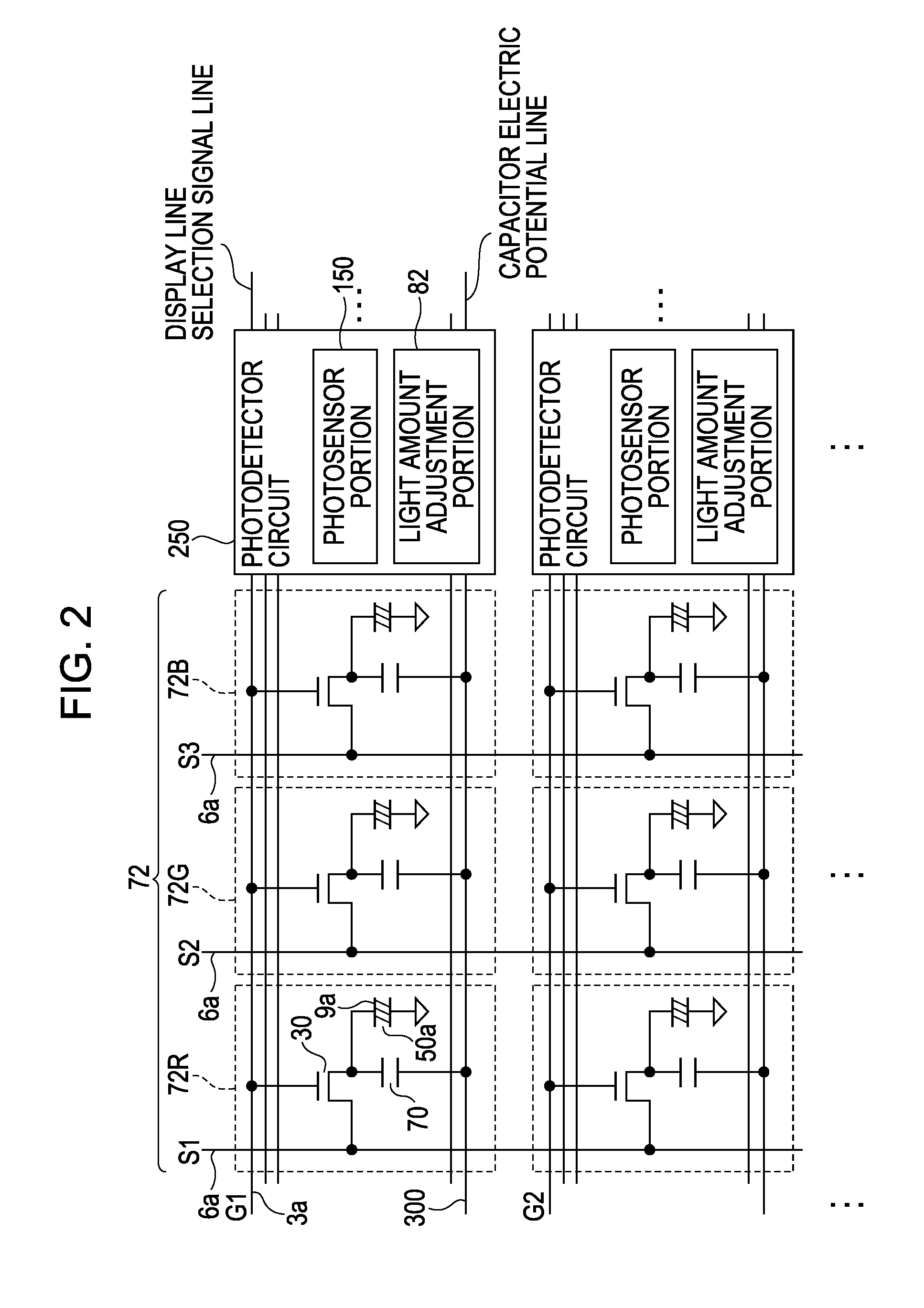
[0126]FIG. 19 is a circuit diagram that shows the configuration of a third example embodiment. As shown in the drawing, in the third example embodiment, one photodetector circuit 250 is arranged for the pixel portions 72 of two lines. Then, the N-th (first, third, fifth, . . . ) display line selection signal lines 3a(N) are also used as a photosensor reset signal line and a photosensor line selection signal line a, and the (N+1)th display line selection signal lines 3a(N+1) are also used as a photosensor line selection signal line b. Thus, an output control TFT 155a and an output control TFT 155b are used as an output control TFT group 155. Note that it is not limited to the arrangement that one photodetector circuit 250 is arranged for the pixel portions 72 of two lines; however, one photodetector circuit 250 may be arranged for the pixel portions 72 of N lines (N is natural number).

[0127]Furthermore, the N-th capacitor electric potential lines 300(N) a...


PUM

PropertyMeasurementUnit
thicknessaaaaaaaaaa
electric currentaaaaaaaaaa
reset voltageaaaaaaaaaa

Abstract

A liquid crystal device includes a plurality of selection lines, a plurality of signal lines, a plurality of pixel portions, a plurality of photosensor portions, a plurality of first power lines, and a plurality of sense lines. The plurality of selection lines are provided in a line direction. The plurality of signal lines are provided in a column direction. The plurality of pixel portions are provided at positions corresponding to intersections of the selection lines and the signal lines. The plurality of photosensor portions are provided in correspondence with a portion of the plurality of pixel portions. The plurality of first power lines are provided in the line direction. The plurality of sense lines are provided in the column direction. Each of the plurality of pixel portions includes a first switching element and a liquid crystal. The first switching element loads a display signal supplied through a corresponding one of the signal lines as a selection signal supplied through a corresponding one of the selection lines is asserted. The liquid crystal exhibits a bright state corresponding to the display signal that is loaded by the first switching element. The portion of the plurality of pixel portions adjust the amounts of light that enter the plurality of photosensor portions. Each of the plurality of photosensor portions includes a photoelectric conversion element, a capacitive element, a second switching element, and a readout portion. The photoelectric conversion element generates an electric current of which the magnitude corresponds to the amount of light received. One end of the capacitive element is electrically connected to the photoelectric conversion element. The second switching element resets the one end of the capacitive element to a reset voltage that is supplied through a corresponding one of the first power lines. The readout portion outputs, to a corresponding one of the sense lines, an output signal of which the magnitude corresponds to a voltage of the one end of the capacitive element. The second switching element is controlled to any one of an on state or an off state on the basis of the selection signal that is supplied through the corresponding one of the selection lines.

Description

BACKGROUND[0001]1. Technical Field[0002]The invention relates to a technology of a liquid crystal device with photodetection function, by which the position of a pointing object, such as finger, is located or the region of the pointing object is detected, and also to a technology of an electronic apparatus provided with the liquid crystal device.[0003]2. Related Art[0004]In liquid crystal devices that are widely used as a display device of an electronic apparatus, or the like, a liquid crystal device having a so-called touch panel function has been suggested. In the touch panel function, a photosensor is arranged for each plurality of pixel portions or for each group consisting of a selected number of pixel portions, and thereby it is possible to display an image using light that is transmitted through the pixel portions and to enter information into the liquid crystal device through the pointing object, such as finger. In the above liquid crystal device, the photosensor detects tha...

Claims


Application Information

Patent Timeline
Patent Type & Authority Applications(United States)
IPC IPC(8): G02F1/133
CPCG02F1/13338G02F2001/13312G06F3/0412G09G2360/148G09G3/3648G09G2300/0465G06F3/042G02F1/13312G06F3/04166
Inventor ISHIGURO, HIDETOKANDA, EIJIOTA, HITOSHI
Owner JAPAN DISPLAY WEST
Why Eureka
Try Eureka