

Method for forming device isolation structure of semiconductor device using annealing steps to anneal flowable insulation layer
a technology of isolation structure and semiconductor device, which is applied in the direction of semiconductor device, semiconductor/solid-state device details, electrical apparatus, etc., can solve the problems of excessive volume shrinkage of semiconductor substrate, undesirable behavior of locos fabrication process, and limiting the size reduction of an active region
- Summary
- Abstract
- Description
- Claims
- Application Information
AI Technical Summary
Benefits of technology
Problems solved by technology
Method used
Image

Examples
Embodiment Construction
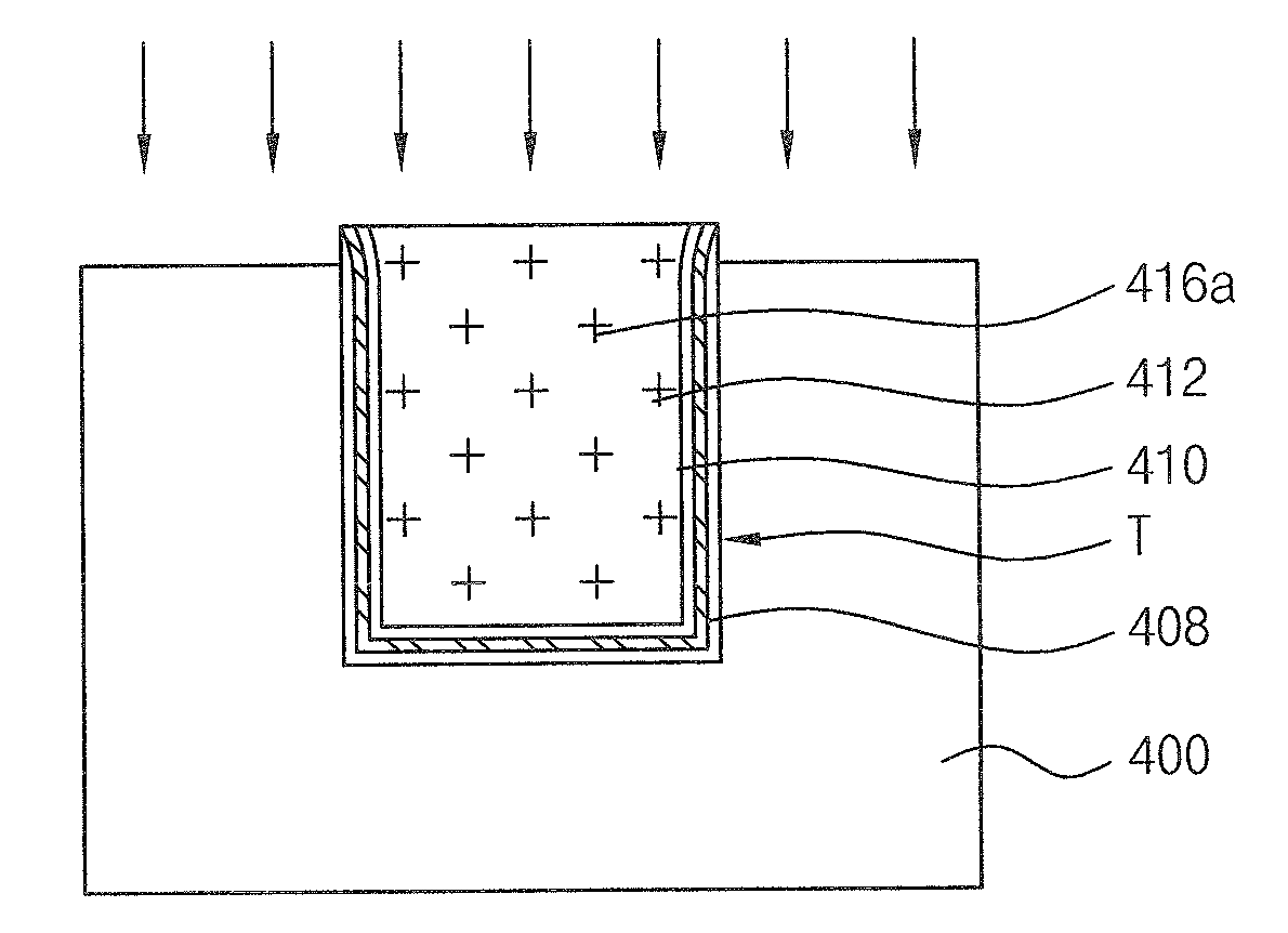
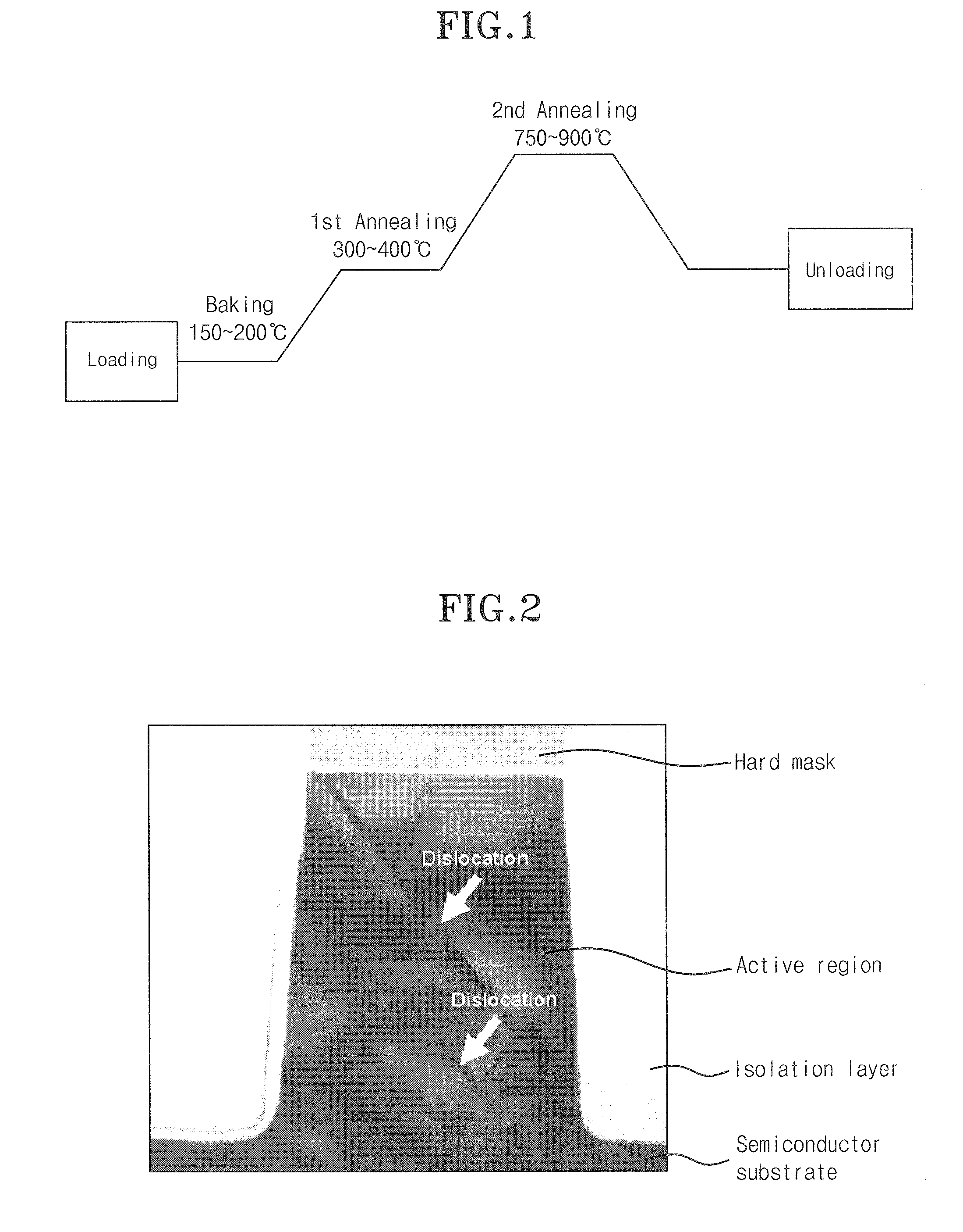
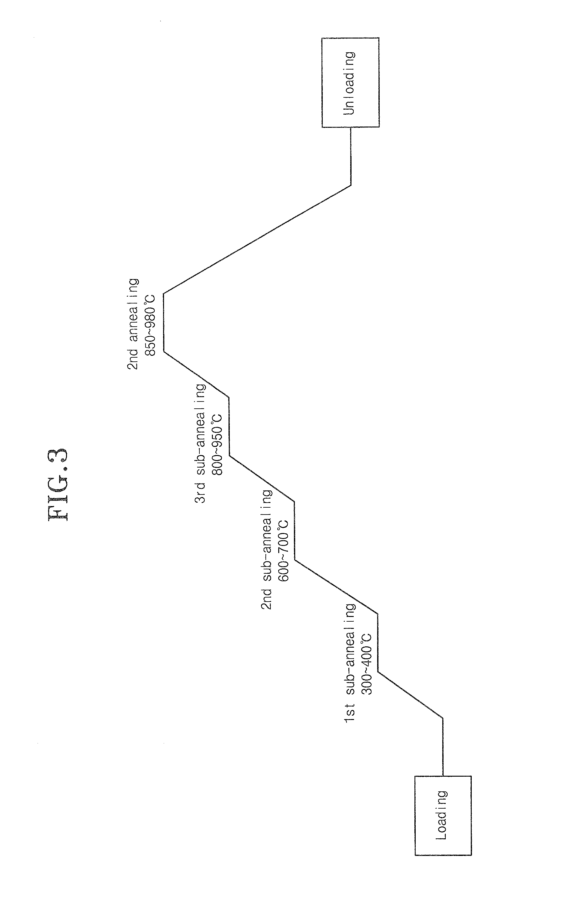
[0046]In an embodiment of the present invention, perhydro-polysilazane is baked, and as a result, the solvent contained in the perhydro-polysilazane volatilizes, by which a PSZ layer is formed. The PSZ layer is annealed at least three times and is thereby oxidated into a SiO2 layer. Then, the SiO2 layer is annealed and is densified thereby.
[0047]Therefore, due to the fact that annealing for oxidating the PSZ layer into the SiO2 layer is implemented at least three times, an abrupt temperature rise can be avoided or at least suppressed while implementing the annealing. Accordingly, in the present invention, the concomitant excessive volume shrinkage of the semiconductor substrate brought about due to the abrupt temperature changes can be minimized.
[0048]Consequently, in the present invention, it is possible to prevent stress from being induced in the semiconductor substrate due to the excessive volume shrinkage. Also, in the present invention, it is possible to prevent defects such as...
PUM
 Abstract
Description
Claims
Application Information