Polygonal area design rule correction method for VLSI layouts

a polygonal area and layout technology, applied in computer aided design, program control, instruments, etc., can solve problems such as inadvertently disrupting the automatic or automated design layout, and inability to meet the requirements of the design process

Inactive Publication Date: 2009-02-05
IBM CORP
View PDF8 Cites 10 Cited by
  • Summary
  • Abstract
  • Description
  • Claims
  • Application Information

AI Technical Summary

Benefits of technology

[0015]The invention further includes a system for optimizing a very large scale integrated (VLSI) circuit design layout that implements an orthogonal polygonal area design rule correcting function for solving maximum/minimum polygonal area violations. The system includes means for receiving a set of data comprising the VLSI circuit design layout, means for identifying polygonal design rule violations in the design layout wherein physical layout edges are represented as variables and means for partitioning identified violating polygons into rectangles in a direction of optimization in the layout, which partitioning includes proportionally adjusting edge distances of each rectangle by

Problems solved by technology

As VLSI technology continues to miniaturize, support hardware and application programs required to reliably print the minimum feature sizes on silicon tend to lag behind technological advancements, further widening sub-wavelength gaps.
But the application of such VLSI design rules may inadvertently disrupt the automatic or automated design layout, to greater or lesser degrees.
Manual layout is a conventional process known to inevitably introduce rules violations due to the difficulty of satisfying large numbers of complex design rules by hand.
Migration is an EDA process that gives rise to a very large number of design rule violations

Method used


Image

  • Polygonal area design rule correction method for VLSI layouts
  • Polygonal area design rule correction method for VLSI layouts
  • Polygonal area design rule correction method for VLSI layouts

Examples


Embodiment Construction

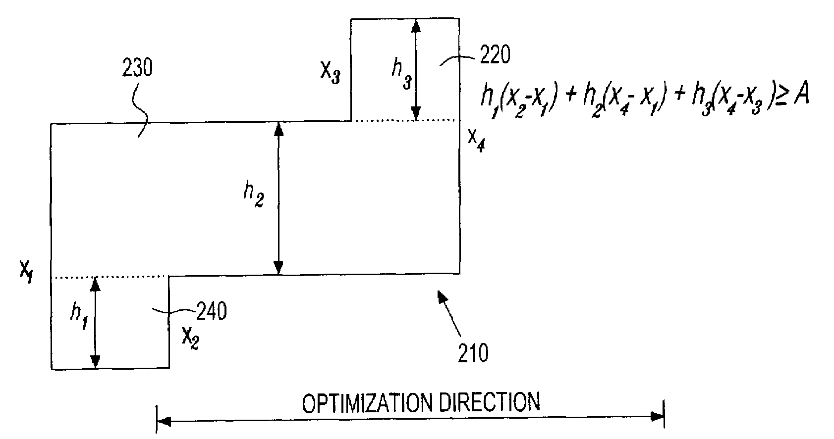
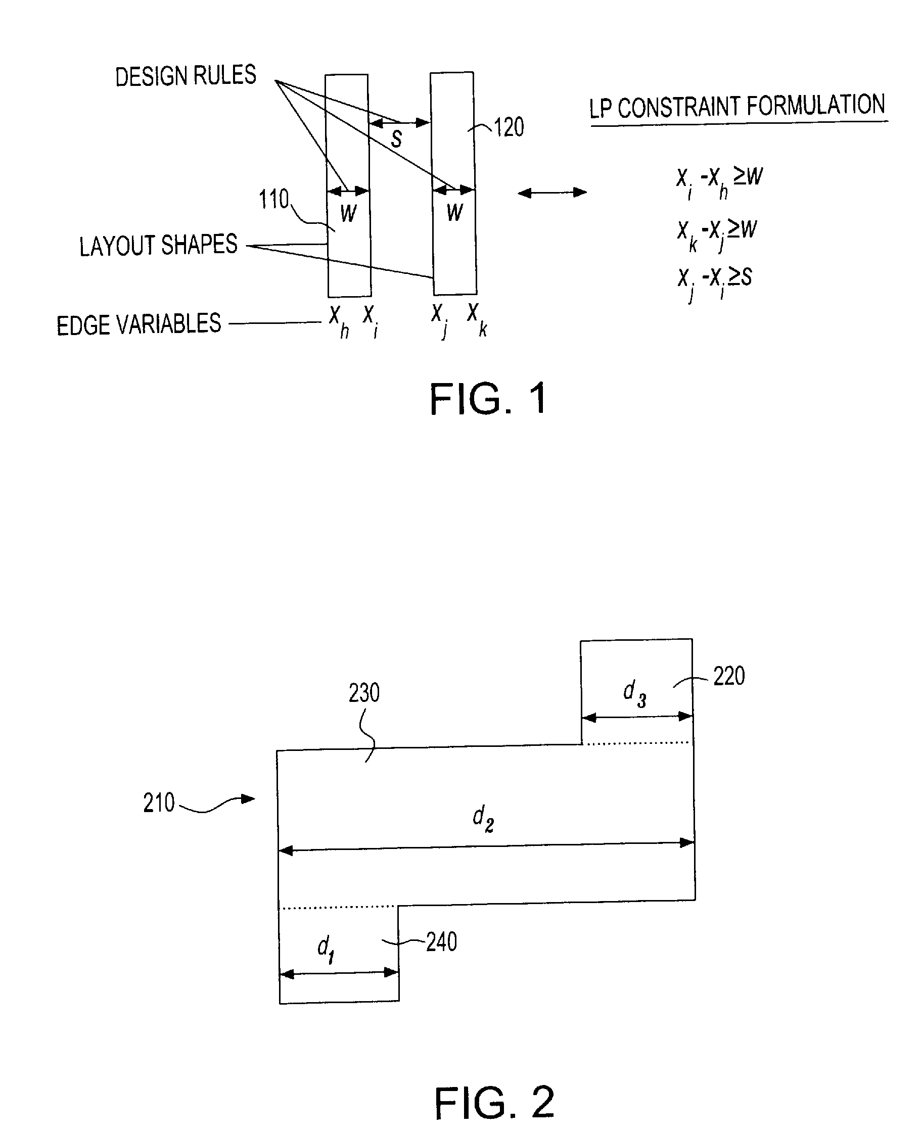
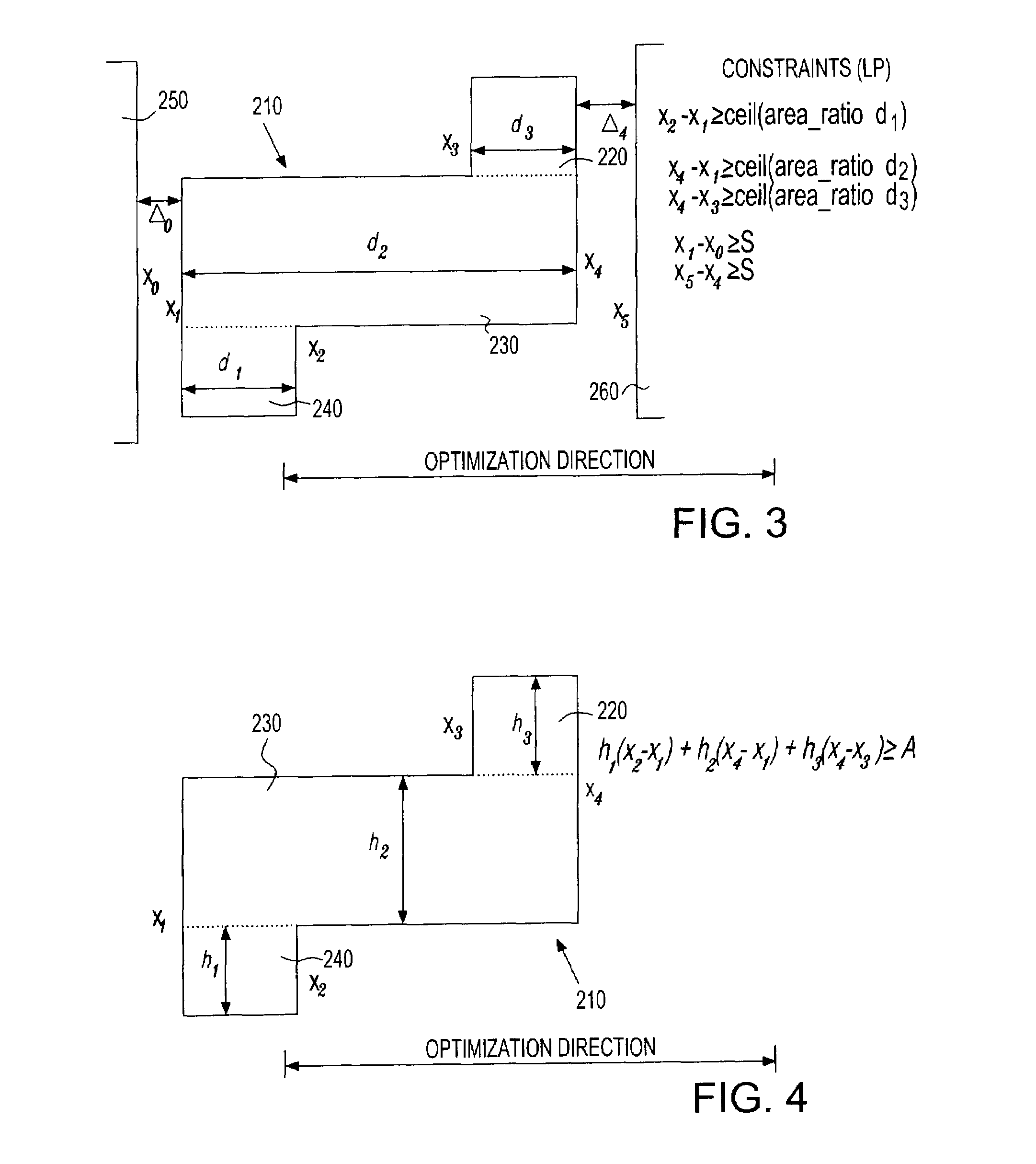
[0024]The inventive method and system set forth and described herein corrects for design rules violations in VLSI design layout modifications, migrations, compactions, etc. The figures and descriptions, however, are intended only as examples, are not exclusive, and should not be interpreted to limit the scope of the invention in any way. The invention is directed to VLSI circuit design processes and automatic design rule correction that includes first finding design rule violations, and then automatically correcting or modifying the design layout to accommodate, correct for, or obviate the design rule violations.

[0025]The inventive method operates in accordance with constraint-based legalization. For example, a first method embodiment corrects for minimum / maximum polygonal area violations while concurrently correcting or preventing most other design rule violation types arising in a migration or compaction process. The physical layout edges are represented as variables, and the desi...


PUM


Abstract

A method of polygonal area design rule correction for use in an electronic design automation tool for governing integrated circuit (IC) design layouts using one-dimensional (1-D) optimization, with steps of analyzing IC design layout data to identify violating polygons, partitioning violating polygons into rectangles in a direction of optimization, formulating an area constraint for each violating polygon to formulate a global linear programming (LP) problem that includes each constraint for each violating polygon and solving the global LP problem to obtain a real-valued solution. A next LP problem is created for each area constraint, and solved. The creating a next and solving the next LP problem and solving are repeated until the last “next LP problem” is solved using constraints and objectives representing sums or differences of no more than two optimization variables.

Description

BACKGROUND OF THE INVENTION[0001]The present invention relates generally to very large scale integrated (VLSI) circuit design, and more particularly relates to an electronic design automation method, and system that implements the method for optimizing a VLSI design, and VLSI design modifications using polygonal area design rule correction.[0002]Characteristics of today's complex very large scale integrated (VLSI) circuit designs have made accelerated processing of graphical design data an essential part of design-to-silicon processes. To achieve profitability, design houses and fabs alike must be capable of processing huge and complicated volumes of design data swiftly. As VLSI technology continues to miniaturize, support hardware and application programs required to reliably print the minimum feature sizes on silicon tend to lag behind technological advancements, further widening sub-wavelength gaps. Such support hardware and application programs, e.g., electronic design automatio...

Claims


Application Information

Patent Timeline
IPC IPC(8): G06F17/50
CPCG06F17/5081G06F30/398
Inventor GRAY, MICHAEL S.GUZOWSKI, MATTHEW T.HIBBELER, JASON D.WALKER, ROBERT F.YUAN, XIN
Owner IBM CORP
Why Eureka
Try Eureka