Organic light emitting diode display device and method of fabricating the same

Inactive Publication Date: 2009-02-19
SAMSUNG MOBILE DISPLAY CO LTD
View PDF19 Cites 55 Cited by
  • Summary
  • Abstract
  • Description
  • Claims
  • Application Information

AI Technical Summary

Benefits of technology

[0007]Embodiments of the present invention are therefore directed to an OLED display device and a method of fabric

Problems solved by technology

Accordingly, since luminance of an EML may be proportional to current supplied to the EML, when a substantially same amount of current is applied to the conventional R, G, and B EMLs, the EMLs of the OLED display device may exhibit non-uniform luminance.
Thus, it may be difficult to obtain a desired color balance or a white balance in th

Method used


Image

  • Organic light emitting diode display device and method of fabricating the same
  • Organic light emitting diode display device and method of fabricating the same
  • Organic light emitting diode display device and method of fabricating the same

Examples


Example

Example 1

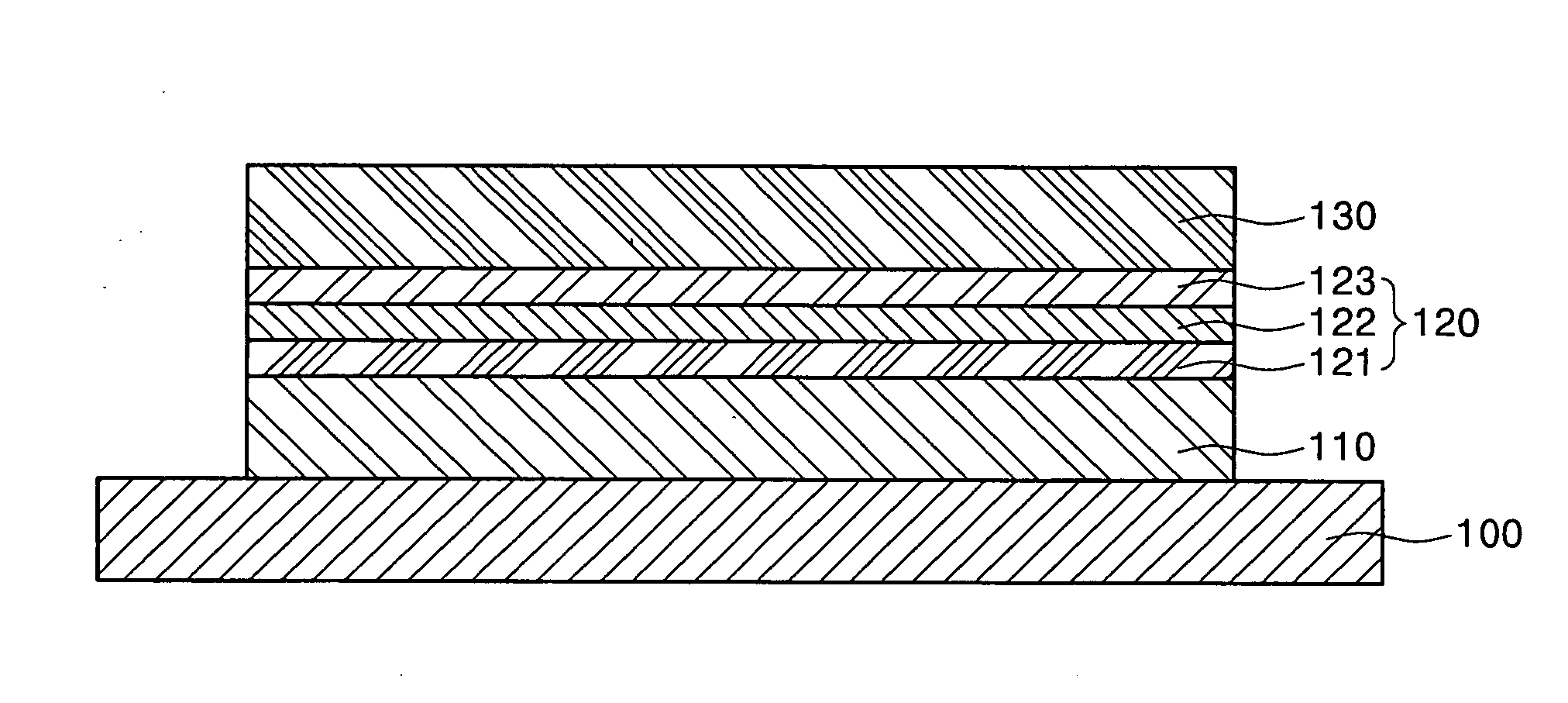
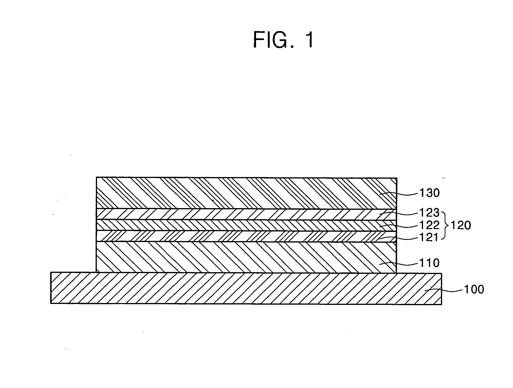
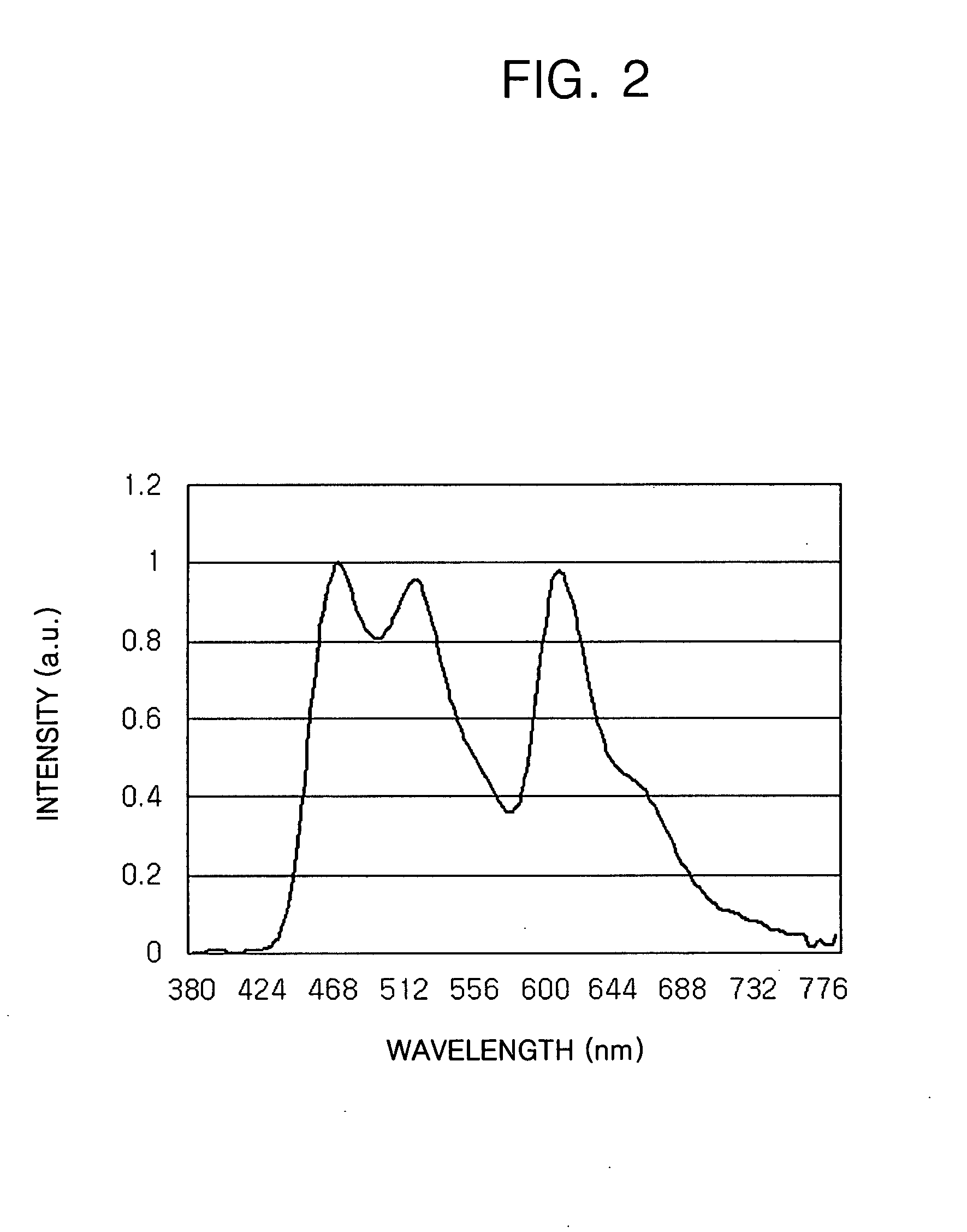
[0036]An ITO layer was formed on a substrate to a thickness of 70 angstroms. An HIL was formed of IDE406 (Idemitsu Kosan Co., Ltd) on the ITO layer to a thickness of 750 angstroms, and an HTL was formed of IDE320 (Idemitsu Kosan Co., Ltd) on the HIL to a thickness of 150 angstroms. A B EML was formed on the HTL to a thickness of 80 angstroms. The B EML was formed of BH232 (Idemitsu Kosan Co., Ltd) as a host material and 10 wt % of BD142 (Idemitsu Kosan Co., Ltd) as a dopant material. A G EML was formed on the B EML to a thickness of 100 angstroms of CBP (UDC, Co., Ltd.) as a host material and 7 wt % of GGD01 (Gracel Display Inc.) as a dopant material. Also, an R EML was formed on the G EML to a thickness of 120 angstroms of CBP (UDC, Co., Ltd.) as a host material and 12 wt % of RD25 (UDC, Co., Ltd.) as a dopant material. An ETL was formed of LG201 (LG Electronics, Inc.) on the R EML to a thickness of 250 angstroms, and an EIL was formed of LiF on the ETL to a thickness of 5...

Example

Example 2

[0037]An OLED display device was prepared according to the method of Example 1, with the exception of using 12 wt %, instead of 10 wt %, of BD142 as a dopant in the B EML.

Example

Comparative Example 1

[0038]An OLED display device was prepared according to the method of Example 1, with the exception of using 8 wt %, instead of 10 wt %, of BD142 as a dopant in the B EML.


PUM


Abstract

An organic light emitting diode (OLED) display device includes a substrate, a first electrode on the substrate, an organic layer on the first electrode, the organic layer including a blue (B) emission layer, a green (G) emission layer, and a red (R) emission layer, the B emission layer including a dopant in an amount of about 10 wt % to about 12 wt %, and a second electrode on the organic layer.

Description

BACKGROUND OF THE INVENTION[0001]1. Field of the Invention[0002]Embodiments of the present invention relate to an organic light emitting diode (OLED) display device and a method of fabricating the same. In particular, embodiments of the present invention relate to an OLED display device capable of uniformly embodying peaks of red (R), green (G), and blue (B) lights.[0003]2. Description of the Related Art[0004]An OLED display device may include a substrate, an anode on the substrate, an emission layer (EML) on the anode, and a cathode disposed on the EML. Application of voltage between the anode and the cathode may trigger injection of holes and electrons into the EML, so the holes and electrons may recombine to generate excitons. Light may be emitted from the EML, while the excitons transition from an excited state to a ground state.[0005]The OLED display device may include a plurality of EMLs to emit different lights, i.e., red (R), green (G), and / or blue (B) lights, so a full-colo...

Claims


Application Information

Patent Timeline
IPC IPC(8): H01L51/52H01J9/02
CPCH01L51/0005H01L51/0009H01L51/001H01L51/0052H01L51/0059H01L2251/558H01L51/007H01L51/0077H01L51/0085H01L51/5016H01L51/5036H01L51/006H10K71/162H10K71/135H10K71/164H10K85/615H10K85/631H10K85/633H10K85/6565H10K85/30H10K85/342H10K50/11H10K2101/10H10K50/125H10K2102/351H05B33/14C09K11/06
Inventor KHO, SAM-ILCHO, JAE-YOUNGLEE, SUN-HEE
Owner SAMSUNG MOBILE DISPLAY CO LTD
Why Eureka
Try Eureka