Circuit and data carrier with radio frequency interface

Active Publication Date: 2009-02-19
NXP BV
View PDF4 Cites 10 Cited by
  • Summary
  • Abstract
  • Description
  • Claims
  • Application Information

AI Technical Summary

Benefits of technology

[0011]The provision of the characteristic features according to the invention provides the advantage that no radio frequency signal generating device is required in order to perform a proper self-test operation of the circuit and of the data carrier, respectively. In comparison to radio frequency signal based testing equipment the present invention allows to use significantly cheaper and simple test equipment for testing purposes, while at the same time no additional pads or connectors are required to perform chip testing operations and to connect the transmission means. In addition, the radio frequency (RF) operational mode of the integrated circuit is not affected by the design according to the invention because the measures according to the invention provide proper operation for radio frequency (alternate current) signals as well as for direct current signals that are fed into the circuit via the two connection pads of the circuit, which connection pads are typically used to be connected with the transmission means. Using direct current signals for testing purposes also provides high immunity against environmental noise.
[0012]Some solutions of the present invention provide the advantage that the input signal fed to the circuit is modulated if it has been detected as the test trigger signal and if the internal functional tests have been carried out with success. Thus, it is very easy to determine w

Problems solved by technology

The known test system, however, is only useful for testing integrated circuits before they are separated from the waver.
Thus, it is not applicable after manufacturing steps of separating the integrated circuits from the waver, fixing them to a substrate and bonding them to an antenna have been carried out.
In practice, this is a big disadvantage, since it has turne

Method used


Image

  • Circuit and data carrier with radio frequency interface
  • Circuit and data carrier with radio frequency interface
  • Circuit and data carrier with radio frequency interface

Examples


Example

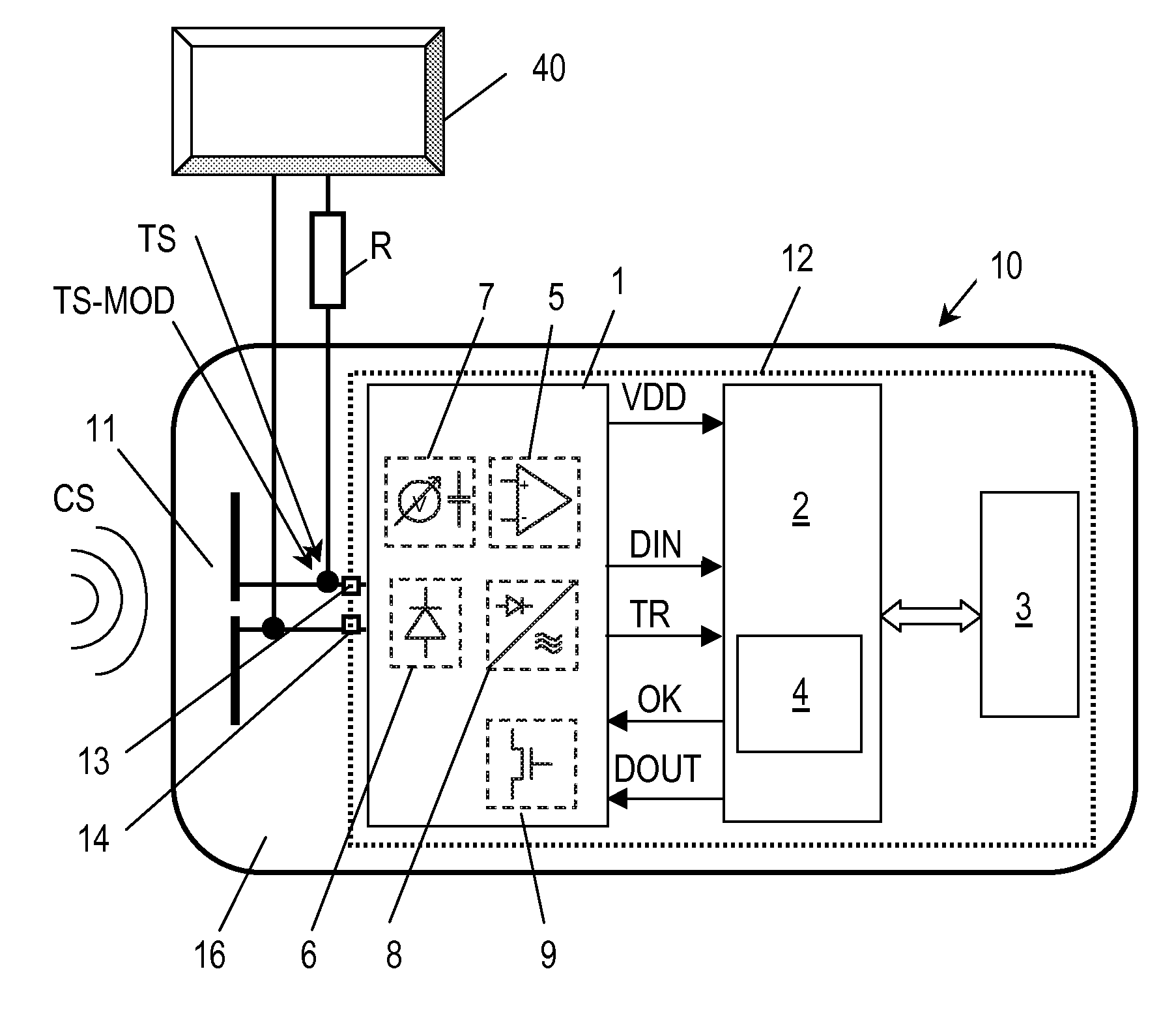
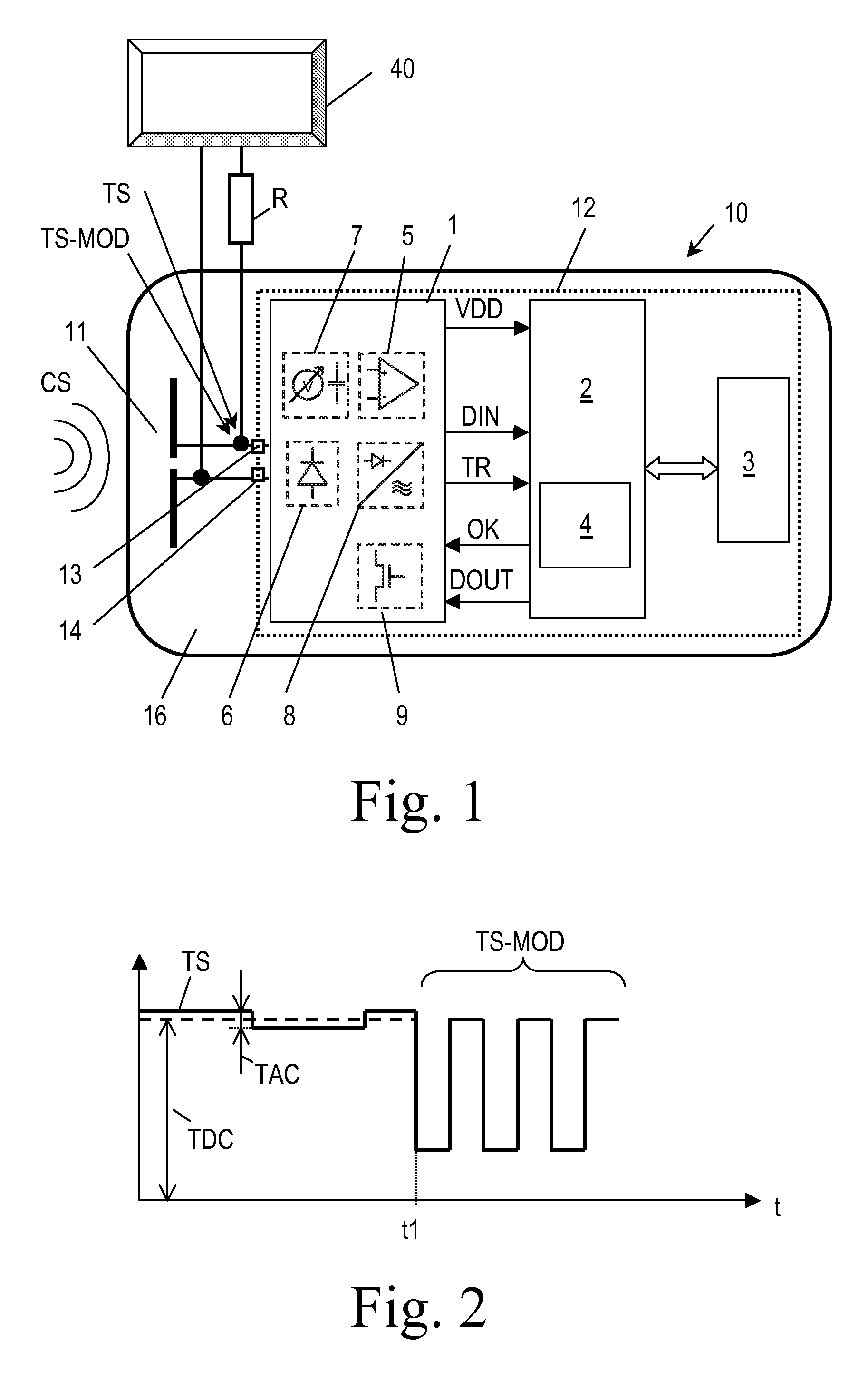
[0022]FIG. 1 shows a schematic block circuit diagram of a general embodiment of a data carrier 10 according to the invention, which data carrier 10 comprises an integrated circuit 12 according to the invention, wherein the integrated circuit 12 is positioned on a substrate 16. The data carrier 10 is configured as a passive transponder and comprises RF transmission means 11 in form of an antenna positioned on the substrate 16, which antenna is designed for receiving in a contact-less manner an electromagnetic RF carrier signal CS from a read / write station not depicted in the drawing. The carrier signal CS can, for instance, have a frequency in the range from a few kHz up to GHz.

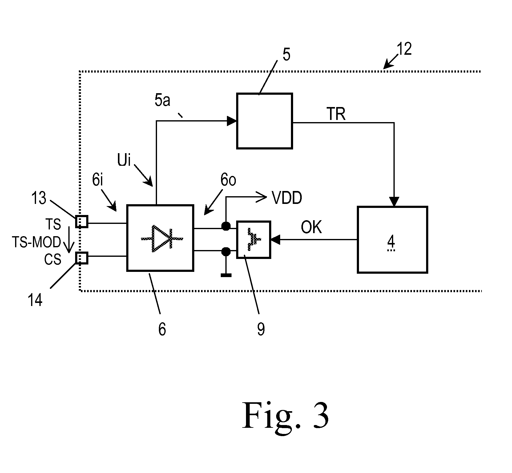
[0023]The RF transmission means 11 are connected to the circuit 12 by means of a first circuit point 13 and a second circuit point 14, which may be configured as connection pads that are wired to the circuit 12. The connection pads may be configured as so called “gold-bumps”, i.e. raised contact-pads that are ...


PUM


Abstract

A circuit (12) comprises a first circuit point (13) and a second circuit point (14), which first circuit point (13) and second circuit point (14) are designed to be connected with RF transmission means (11) being designed for receiving in a contact-less manner a carrier signal (CS) from a read/write station and for feeding the circuit (12) with the received carrier signal (CS). The circuit (12) further comprises circuit testing means (4) being designed to carry out functional tests of the circuit (12) and to output a modulated response signal (TS-MOD) via the first and second circuit points (13, 14) only if the functional tests have been successful. The circuit (12) further comprises test trigger signal detecting means (5) being designed for detecting a test trigger signal (TS) that is applied across the first circuit point (13) and the second circuit point (14), wherein the test trigger signal detecting means (5) are designed to trigger the circuit testing means (4) to carry out the functional tests if they detect the test trigger signal (TS).

Description

FIELD OF THE INVENTION[0001]The invention relates to a circuit for a data carrier.[0002]The invention further relates to a data carrier with a circuit according to the preceding paragraph.BACKGROUND OF THE INVENTION[0003]Recent developments in industry have shown that Radio Frequency Identification Systems (RFID-systems) are becoming an integrated part of logistics and transportation applications. On one hand such RFID-systems typically comprise at least one data carrier, which data carrier comprises an integrated circuit and transmission means that are connected to the integrated circuit. On the other hand such RFID-systems comprise a read / write station, also known as RFID reader, that provides a Radio Frequency (RF) carrier signal for the purpose of powering the integrated circuit of the data carrier and for exchanging data with said integrated data carrier by the aid of the RF carrier signal in a contactless manner. Due to increasing demand for long distance RFID-systems the doma...

Claims


Application Information

Patent Timeline
IPC IPC(8): G01R31/3187
CPCG01R31/2884G06K19/07749G01R31/31701G01R31/3025G01R31/28G01R31/303
Inventor BRANDL, ROLANDBERGLER, EWALDSPINDLER, ROBERT
Owner NXP BV
Why Eureka
Try Eureka