Method of Manufacture and Identification of Semiconductor Chip Marked For Identification with Internal Marking Indicia and Protection Thereof by Non-black Layer and Device Produced Thereby

a technology of semiconductor chips and internal markings, applied in the direction of semiconductor devices, semiconductor/solid-state device details, electrical apparatus, etc., can solve the problems of high cost of x-ray inspection, and achieve the effect of reducing inspection cost and alleviating safety concerns

Inactive Publication Date: 2009-02-26
QUALCOMM INC
View PDF98 Cites 20 Cited by
  • Summary
  • Abstract
  • Description
  • Claims
  • Application Information

AI Technical Summary

Benefits of technology

[0012]An object of this invention is to replace the process of X-ray inspection of integrated circuit chips to reduce the cost of inspection and to alleviate the concerns pertaining to safety issues.

Problems solved by technology

It is expensive to use X-ray inspection and personnel operating the inspection apparatus always need to be concerned the safety factors involved with the use of X-rays.

Method used


Image

  • Method of Manufacture and Identification of Semiconductor Chip Marked For Identification with Internal Marking Indicia and Protection Thereof by Non-black Layer and Device Produced Thereby
  • Method of Manufacture and Identification of Semiconductor Chip Marked For Identification with Internal Marking Indicia and Protection Thereof by Non-black Layer and Device Produced Thereby
  • Method of Manufacture and Identification of Semiconductor Chip Marked For Identification with Internal Marking Indicia and Protection Thereof by Non-black Layer and Device Produced Thereby

Examples


Embodiment Construction

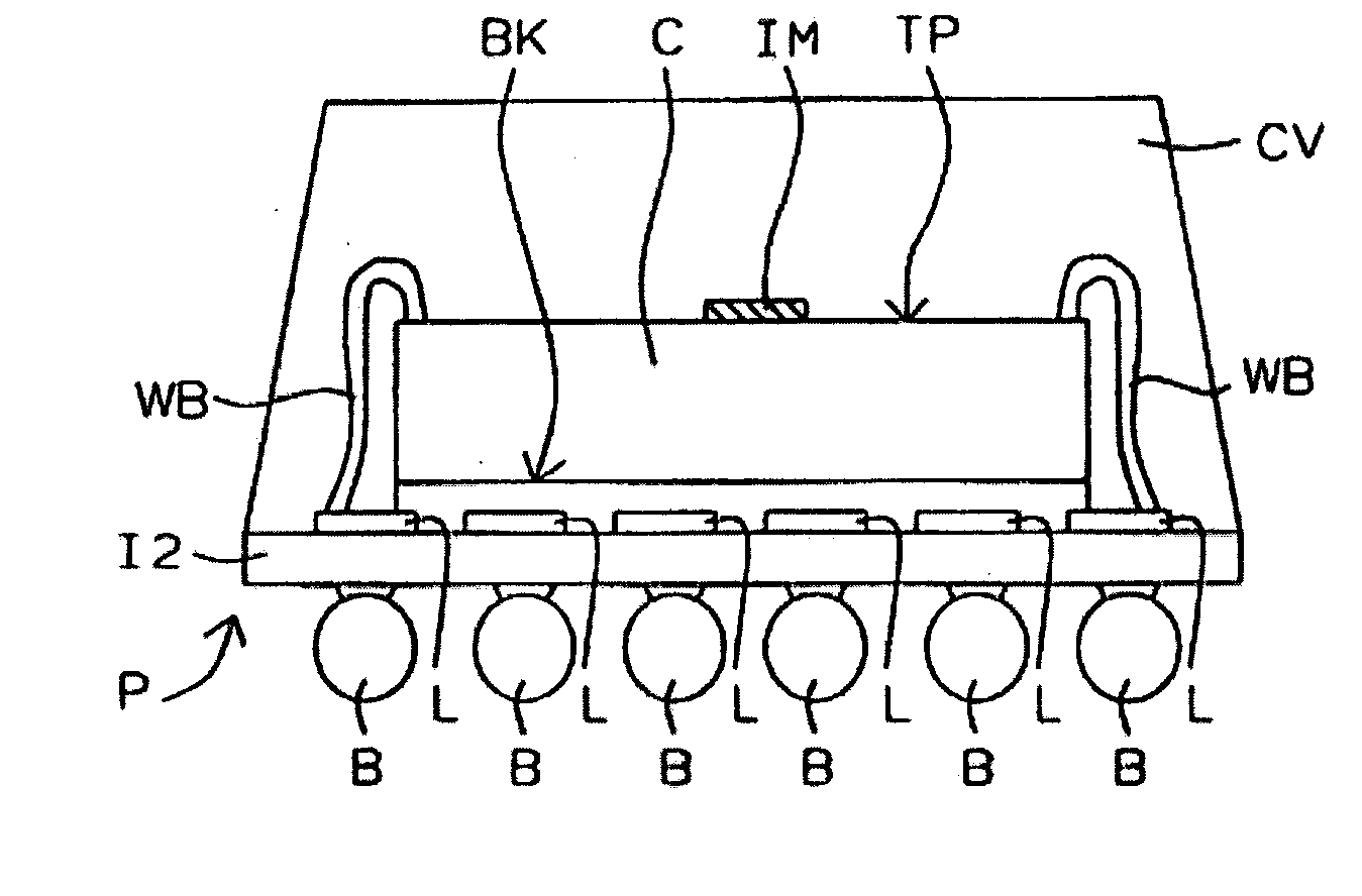
[0089]FIG. 31 shows a first way of marking a package P1. Package P1 includes a chip CH1, a black layer BL, a non-black protection layer PL1 and externally applied indicia comprising a top mark TM. The black layer BL is formed on the top surface of the chip CH1. The non-black, protection layer PL3 is formed on the top surface of the black layer BL. The black layer BL may be pigmented by impregnating a molding compound with carbon to make the black layer BL light absorbing. A laser-written, opaque top mark TM is formed on the exterior of the non-black, protection layer PL. There is a problem with an externally-applied indicia comprising top mark TM which is easily remarked since the laser mark TM is on the top external surface of the chip package P1. Balls BL of a Ball Grid Array (BGA) are provided for electrical connection of circuits on the chip CH1 and mechanical connection of the chip CH1 to a connection board (not shown) is shown on the lower surface of the chip CH1.

[0090]FIG. 32...


PUM


Abstract

An electronic integrated circuit has a planar front surface and a planar backsurface. Internal marking indicia identification are marked upon an marking surface on the exterior surface of the chip. The internal identification indicia on the chip surface are protected against remarking by a non-black, colored, optically transmissive layer, so the indicia are visible through the optically transmissive material. Electrical interconnection means connect to the electrical contact site through the package. There is least one electrical contact site on an exterior surface of the chip.

Description

[0001]This application is a continuation of application Ser. No. 09 / 523,990, filed on Mar. 13, 2000, now pending.BACKGROUND OF THE INVENTION[0002]1. Field of the Invention[0003]This invention relates to semiconductor packages and more particularly to materials and methods employed in packaging thereof.[0004]2. Description of Related Art[0005]Encapsulation materials for semiconductor packages are colored black to protect the contents thereof from light. Thus X-rays must be used for the inspection after encapsulation. It is expensive to use X-ray inspection and personnel operating the inspection apparatus always need to be concerned the safety factors involved with the use of X-rays.[0006]The continued trend toward miniaturization of electronic and electrical systems requires a reduction in the overall size of the semiconductor device packages that are employed therein. Thus, small size packages having excellent reliability, and multi-function capability are required.[0007]U.S. Pat. N...

Claims


Application Information

Patent Timeline
Patent Type & Authority Applications(United States)
IPC IPC(8): H01L23/488H01L23/544
CPCH01L23/3114H01L23/3157H01L2924/10253H01L2224/73215H01L2224/32225H01L23/544H01L25/0657H01L2223/54413H01L2223/54433H01L2223/54486H01L2224/48091H01L2225/06517H01L2225/0652H01L2924/01078H01L2924/01079H01L2924/15311H01L24/48H01L2224/73265H01L2924/00014H01L2924/00H01L2924/14H01L2924/181H01L2924/1815H01L2924/00012H01L2224/45099H01L2224/45015H01L2924/207
Inventor LIN, MOU-SHIUNG
Owner QUALCOMM INC
Why Eureka
Try Eureka