

Nitride-based semiconductor laser device and method of manufacturing the same
- Summary
- Abstract
- Description
- Claims
- Application Information
AI Technical Summary
Benefits of technology
Problems solved by technology
Method used
Image

Examples
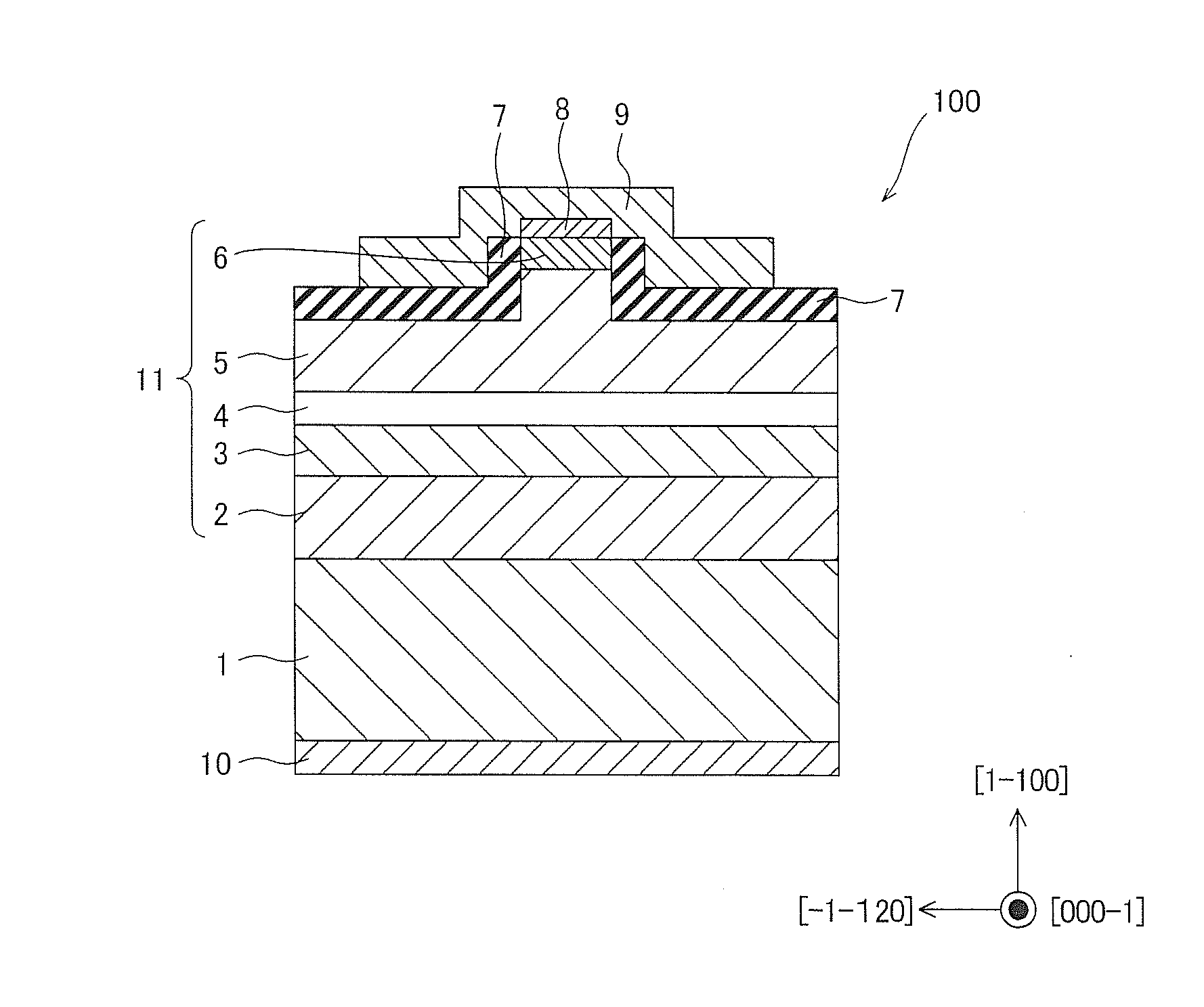
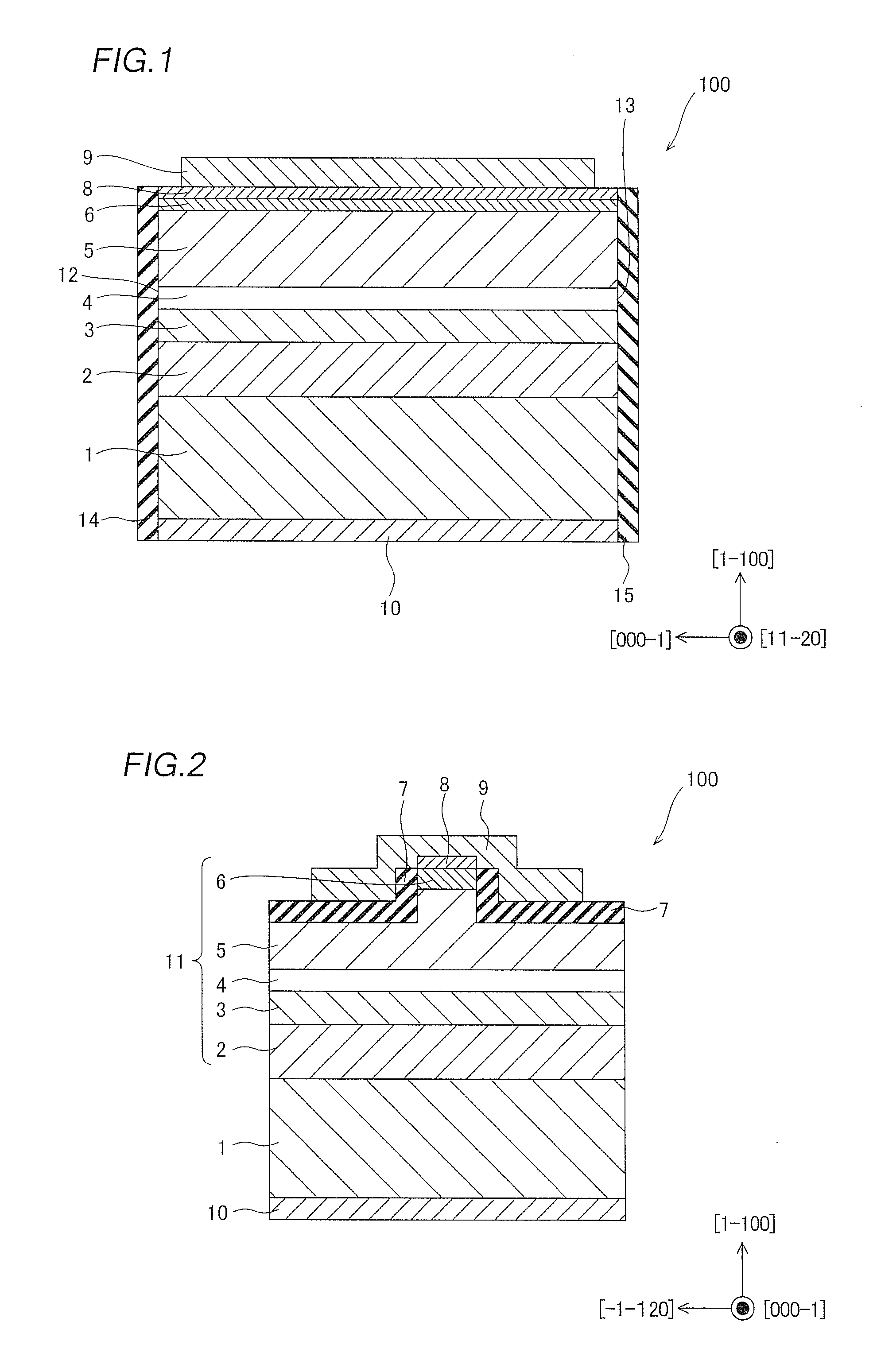
first embodiment
Modification of First Embodiment
[0065]A modification of the first embodiment will be now described.
[0066]According to the modification of the first embodiment, Al or In composition of AlGaN, InGaN or the like forming an n-type cladding layer 33, an emission layer 34 and a p-type cladding layer 35 is different. More specifically, while Al0.07Ga0.93N is employed as the n-type cladding layer 33 and the p-type cladding layer 35 according to the aforementioned first embodiment, Al0.03Ga0.97N is employed as the n-type cladding layer 33 and the p-type cladding layer 35 according to the modification of the first embodiment. The doses and carrier concentrations of the n-type cladding layer 33 and the p-type cladding layer 35 according to the modification of the first embodiment are similar to those of the aforementioned first embodiment.
[0067]An n-type carrier blocking layer made of n-type Al0.10Ga0.90N and an n-type light guide layer made of n-type In0.05Ga0.95N are employed as the emission...
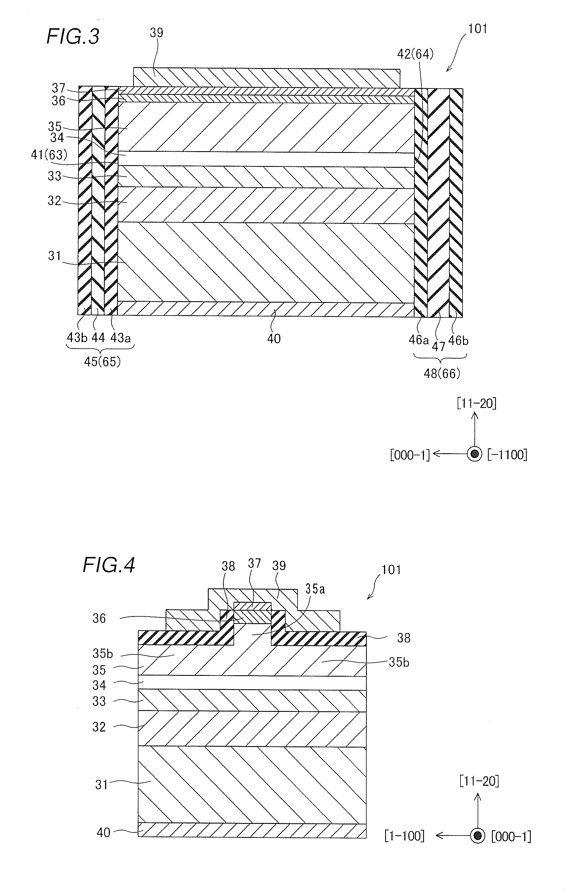
second embodiment
Modification of Second Embodiment
[0075]A modification of the second embodiment will be now described.
[0076]According to the modification of the second embodiment, a structure similar to that of the aforementioned modification of the first embodiment is applied to the aforementioned second embodiment and the semiconductor laser structure similar to that of the aforementioned modification of the first embodiment is formed on an n-type GaN (1-100) plane misoriented substrate 51 having a thickness of about 100 μm and doped with oxygen, having a carrier concentration of about 1×1018 cm−3, as shown in FIGS. 5 and 6.
[0077]The remaining structure of the GaN-based semiconductor laser device according to the modification of the second embodiment is similar to that of the GaN-based semiconductor laser device according to the aforementioned modification of the first embodiment.
[0078]According to the modification of the second embodiment, In composition contained in a MQW active layer is higher ...
third embodiment
Modification of Third Embodiment
[0091]A modification of the third embodiment will be now described.
[0092]According to the modification of the third embodiment, a structure similar to that of the aforementioned modification of the first embodiment is applied to the aforementioned third embodiment and a GaN-based semiconductor laser device provided with irregularities 62 on regions other than regions formed with an optical waveguide of a light emitting surface 63 and a light reflecting surface 64 is formed as shown in FIG. 7, dissimilarly to the aforementioned modification of the first embodiment.
[0093]The remaining structure of the GaN-based semiconductor laser device according to the modification of the third embodiment is similar to that of the GaN-based semiconductor laser device according to the aforementioned modification of the first embodiment.
[0094]According to the modification of the third embodiment, In composition contained in a MQW active layer is higher than that of the ...
PUM
 Abstract
Description
Claims
Application Information